|
|
Bachelor's Degree in Telecommunications Systems and in Network Engineering |
|
|
|
||
|
|
4-digit BCD counter modulo 3600 (minutes and seconds counter) |
|
|
|
||
| 1. Specifications | Planning | Developing | Test functional | Test gate-level | Report | Prototype |
Design the Counter_BCD_MMSS the symbol of which is drawn in Fig. 1. It is a 4-digit BCD counter module 3600 divided in two chained SS (modulo 60) and MM (modulo 60) synchronous counters.
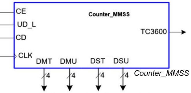 |
| Fig 1. Symbol. |
| Specifications | 2. Planning | Developing | Test functional | Test gate-level | Report | Prototype |
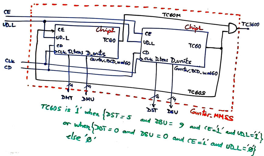
As represented in Fig. 2, Counter_MMSS can be invented using plan C2 expanding Counter_BCD_mod60 devices.
 |
|
Fig 2. Inventing the Counter_MMSS (visio) requires chaining Counter_BCD_mod60 blocks for counting seconds and minutes. |
Project location:
C:\CSD\P8\Counter_MMSS\(files)
| Specifications | Planning | 3. Developing | Test functional | Test gate-level | Report | Prototype |
Example file translation of schematics above in Fig. 2: Counter_MMSS.vhd, Counter_BCD_mod60.vhd, Quad_MUX_2.vhd, and copy the Counter_mod16.vhd from its plan Y tutorial Counter_mod16.
Fig. 4 and Fig. 5 show RTL and technologies views for a target chip MAX10 10M50DAF484C7.
  |
|
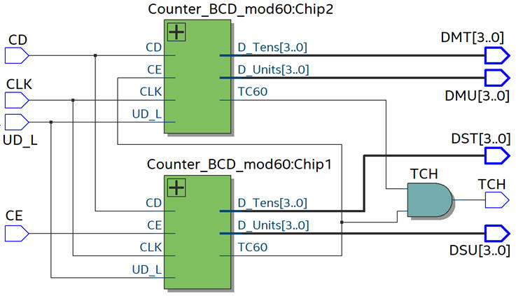
Fig 4. Top Counter_MMSS RTL circuit and its component Counter_BCD_mod60. built chaining basic Counter_mod16. |
Total number of registers D_FF is 16. Total logic elements is 79.
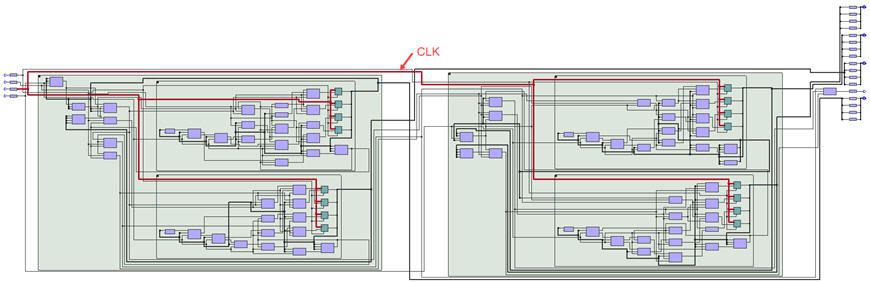 |
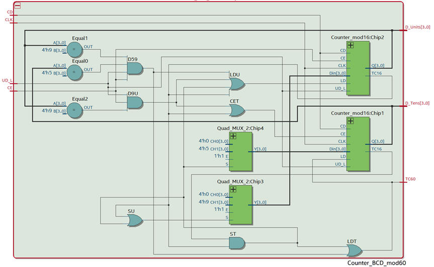
Fig. 5. Technology view emphasising how the CLK signal is distributed to all 16 D_FF. (pdf) |
| Specifications | Planning | Developing | 4. Test functional | Test gate-level | Report | Prototype |
We need to drive CLK, CD, CE and UD_L in the usual way.
Generate from Quartus Prime the VHDL testbench fixture skeleton. Rename it and move it to the project folder.
Copy from this example file Counter_MMSS_tb.vhd only the stimulus activity described in the two processes and also the constant CLK_Period.
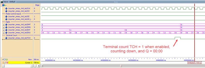
Start and run a functional simulation project using ModelSim to verify that the device operates correctly. Let us try one mode of operation at a time. For instance, Fig. 6 shows how the circuit is counting down. It need a time of 3600·CLK_Period to complete all counting range.
 |
|
Fig. 6. Simulation results. |
| Specifications | Planning | Developing | Test functional | 5. Test gate-level | Report | Prototype |
| Specifications | Planning | Developing | Test functional | Test gate-level | 6. Report | Prototype |
Follow this rubric for writing reports.
| Specifications | Planning | Developing | Test functional | Test gate-level | Report | 7. Prototype |
We built and use this module in several training and demonstration designs:
A) Timer_MMSS, P8 highlighted project as the main component Counter_BCD_MMSS of the datapath.
B) Prototype in a legacy DE0 board. Target chip: Cyclone III 3C16F484C6N
| Home Term 26/27-Q1 Contact Products Electronic devices and companies Software Books Magazines Instruments DEE Library EETAC DEEL |

|
|
| Web activa des de 09/2001, @ F. J. Robert, Web editat amb Microsoft Expression Web 4. El contingut és un complement als materials d'estudi del curs Circuits i Sistemes Digitals disponibles al campus digital Atenea. Llicència:Reconeixement 4.0 Internacional de Creative Commons |