Legacy hardware: Altera NIOS board |
| Prototype specifications | Planning | Development and Test & Measurements |
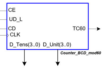
Let us adapt the Counter_BCD_mod60 represented in Fig. 1 for the Altera NIOS board populated with an obsolete Altera APEX 20KE FPGA.
This board was mainly designed for experimenting with soft-processors embedded in FPGA. It contains by factory default the NIOS 32-bit microcontroller and all the documentation is related to this architecture. Newer boards of the same kind from Intel-Altera uses advanced NIOS-II or ARM microcontrollers. In our introductory CSD course, we simply will use the training board for instantiating logic circuits from Chapter 1 (combinational) and Chapter 2 (sequential) as we are doing with all other platforms. The use of embedded soft and hard processors in FPGA is left for advanced courses in digital systems as a viable design alternative to commercial microcontroller chips, beyond our Chapter 3.
 |
|
Fig. 1. Symbol of the basic counter. |
We will add some additional features to the top design, such:
- Switch for selecting two CLK frequencies for fast (20 Hz) and slow (1 Hz) counting (Sel_CLK_freq)
- Count enable switch (CE)
- Switch for counting up or down (UpD_L)
- Switch for selecting manual or internal oscillator CLK signal (Sel_pulse)
- Switch for selecting raw CLK input from the push-button (CBL_L) or debounced and filtered pulse (Sel_filter)
- TC60 LED indicator
- Tens and Units 7-segment displays to show the current counter count.
- LED ticking at 1 Hz (LED_CLK_1Hz_SQ)
- LED for indicating manual CLK (LED_CLK_pulse)
This is the time for reviewing the NIOS board hardware and software details. Unfortunately, Intel - Altera has long ago discontinued such product, thus we will use software and documentation from the board's CD and DVD. Review:
-Basics of CPLD and FPGA.
- APEX20K200EFC484-2X architecture. Number of logic elements available for experimetation.
- How to configure the APEX device in the NIOS board environment. JTAG configuration (*.sof RAM file). SOPC Builder platform for accessing the board's configuration (*.flash file) flash memory.
- Electronic schematic. Which resources are easy to use in our introductory level course? User switches, LED, push-buttons, 7-segment displays, etc.
| Prototype specifications | Planning | Development and Test & Measurements |
We will follow the steps:
1. Develop and test functionally the application in Quartus Prime. Project folder:
C:\CSD\LEGACY\NIOS\Counter_BCD_mod60_top\(files)
2. Copy VHDL source files in the Window 7 VM for resynthesising using Quartus II 9.0, where we still can find the APEX target chip. Assign pins and generate the configuration files: *.sof, *.pof, .hexout, .flash.
C:\CSD\NIOS\Counter_BCD_mod60_top\(files)
3. Use JTAG interface to check the *.sof. This a fast method, very convenient, but volatile; when powering off and on the board or clicking its RESET pushbutton, the FPGA is is configured again with the default application.
4. Use NIOS SOPC Builder tools to configure permanently the flash memory with our application. This is a slow process, thus better to do it only when the application is fully operational.
The following fully annotated plan C2 schematic is proposed for this adaptation to the FPGA board.
 |
|
Fig. 2. Counter_BCD_mod60_top adaptation. |
| Prototype specifications | Planning | Development and Test & Measurements |
Developing will be integrated with testing for each of the four planned steps. We can only go ahead when the current steps works correctly.
1. Quartus Prime project
To complete the synthesis and functional testing of our application, we can develop the project using our current Quartus Prime EDA. At this stage we can select any target FPGA.
The only circuit to which pay some attention is the CLK_Generator, to be adapted to the 33.333 MHz quartz crystal available in the NIOS board. The first frequency divider is N1 = 166665.
This is the list of VHDL files included in the design: Counter_BCD_mod60_top.zip.
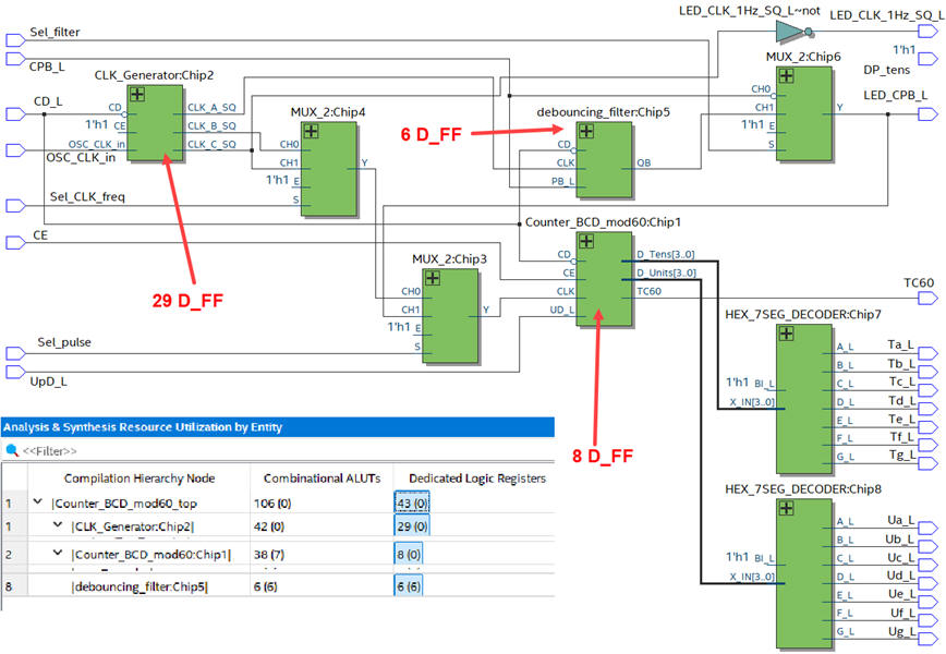 |
| Fig. 3. No complications are expected in this RTL view because the main project is our standard Counter_BCD_mod60 used in many other CSD applications for counting minutes or seconds. We are expecting 43 D_FF. |
2. Quartus II project. Pin assignment, configuration files
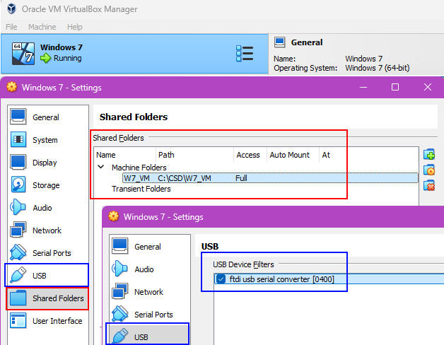
In this next stage, we can switch computers and tools to be able to target the obsolete APEX 20KE device. Let us use the VM running Windows 7 and Quartus II version 9.0. Use the shared drive
 |
|
Fig. 4. Shared folder C:\CSD\VM_W7 and USB to serial adapter available in Window 7. |
Let us start a new VHDL project for the APEX FPGA considering all the imported VHDL files. If we have to use the same environment for different legacy tools, it is convenient to organise separated projects. For instance:
C:\CSD\NIOS\Counter_BCD_mod60_top\(files)

Once the project synthesised with no errors, we can use the pin planner tool to assign pins as shown in Fig. 5 and synthesise the project.
  |
|
Fig. 5. Pin assignments can be saved in a file Counter_BCD_mod60_top.csv ready to be imported to the Quartus II project. |
In this way, the generated output file Counter_BCD_mod60_top.sof will be ready for programming the FPGA in the next step.
3. JTAG, *.sof
Let us use the MAX-II micro kit as an USB blaster cable connecting it as indicated in Fig. 6.
 |
|
Fig. 6. Using the MAX-II micro kit as a USB blaster cable for configuring the APEX FPGA. |
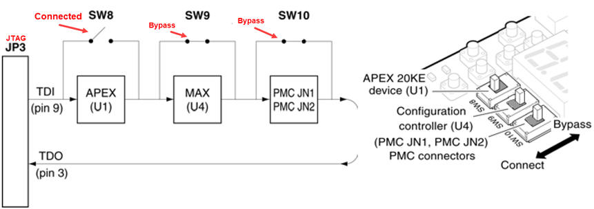
Be aware of connecting the JTAG interface for the U1 APEX 20KE FPGA. Bypass the other chips.
 |
|
Fig. 7. Using the MAX-II micro kit as a USB blaster cable for configuring the APEX FPGA. |
When ready, use the programmer tool installed in your Windows 11 computer to locate the target chip where to upload the configuration file.
|
|
|
Fig. 8. Programmer application. It also works as an standard alone application. |
This FPGA configuration step can be executed directly from the programmer as an standard-alone application. Let us use the *.sof file for the FPGA RAM produced above in Quartus II. The extension .sof stands for SRAM Object File. The APEX will be detected in the JTAG chain.
 |
|
Fig. 9. The APEX is the only programmable device attached to the JTAG chain. |
Check that the NIOS board works as expected running the Counter_BCD_mod60_top configuration.
Check how the Debouncing_filter FSM is required (Sel_filter switch) when clicking the push-button for applying CLK pulses to the counter.
There is another programmable chip available in the NIOS board: the U4 CPLD EPM7064AE. However, it contains the general NIOS board configuration controller that accepts *pof files; better not to touch it. In order to write non-volatile applications on the APEX FPGA we have to use the external flash memory. This is going to be the goal of the next section.
4. Flash memory *.flash
At this stage, the idea is to save permanently the FPGA configuration in the flash memory. It contains the default factory NIOS microcontroller application and the user application.
We have to use the SOPC Builder platform conceived mainly for compiling and debugging C code for the NIOS microcontroller. However it also includes a monitor program (GEMS) and specific utilities for interfacing the board. Therefore, it is possible to write a user application in the flash memory section to be immediately uploaded into the FPGA on power on.
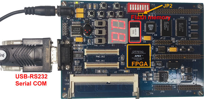 |
|
Fig. 10. USB-COM connection for downloading the configuration program into the flash memory. |
The platform SOPC Builder SDK is installed along with Quartus II version 9.0 under a folder named "Excalibur".
 |
|
Fig. 11. SOPC Builder location. |
1. Connect the USB cable serial port
We use a USB-Serial COM cable adapter to create a COM port for our computer.
 |
|
Fig. 12. USB to serial COM adapter cable. |
We can configure such port once detected by Windows 7.
 |
| Fig. 13. USB serial port COM5 configuration. |
2. Check the board resources. From the SOPC Builder console:
Let us assume that the serial cable is connected to COM5. Type this command to begin communicating with the development board and check the boards resources:
[SOPC Builder]$ nios-run -p com5 -t
 |
|
Fig. 14. Checking the basic resources available on board using command nios-run to establish communication. |
3. Convert the *.hexout file to the *.flash
We have to be sure that the Quartus II project is synthesised with the option to generate the *.hexout file.
 |
|
Fig. 15. Setting the option hexadecimal (Intel-format) output file (hexout). |
Thus, we can convert it to flash type ready for downloading it into the NIOS board using this command available from the SOPC Builder console:
[SOPC Builder]$ hexout2flash Counter_BCD_mod_60_top.hexout
 |
Fig. 16. The file Counter_BCD_mod60_top.hexout.flash is listed. |
4. Use nios-run command from SOPC Builder console to download the flash configuration file
This command is for writing the flash memory.
[SOPC Builder]$ nios-run -z -x -p com5 Counter_BCD_mod60_top.hexout_flash
Writing to this flash device is a very slow process, it takes many minutes:
|
|
|
Fig. 17. Slow downloading process for writing the FPGA configuration flash memory. |
And, now it is time to check the new permanent configuration. You can use the jumper JP2 cap to bypass this application and go back to the factory NIOS setup.
 |
|
Fig. 18. NIOS board running the Counter_BCD_mod60 application stored permanently in the configuration flash. |


