|
|
Bachelor's Degree in Telecommunications Systems and in Network Engineering |
|
| Analysis and design tutorials | Analysis and design assignments | Prototypes | Exam 1 | Exam 2 | Questions and assessment |
CSD EXA1: midterm exam examples and solution ideas |
2526Q2
Problem 1
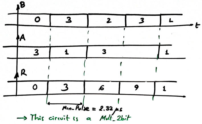
1. Timing diagram observing the truth table. A, B are 2-bit radix-2 numbers.
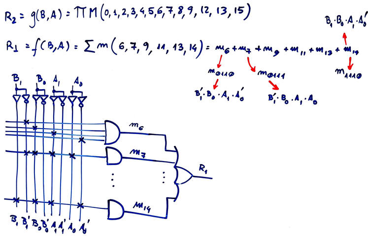
2. Maxterms and minterms.
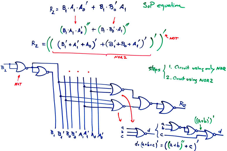
3. Only-NOR2
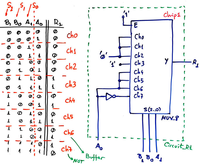
4. Apply to output R1 the MoM presented in lecture L3.4.
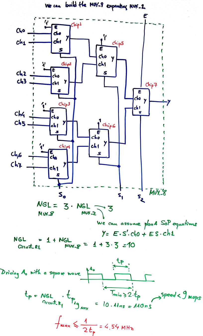
5. We can calculate Circuit speed for the output with the longest propagation path. R2 solved as in 3 has NGL = 7. For instance considering R1 solved as in 4,
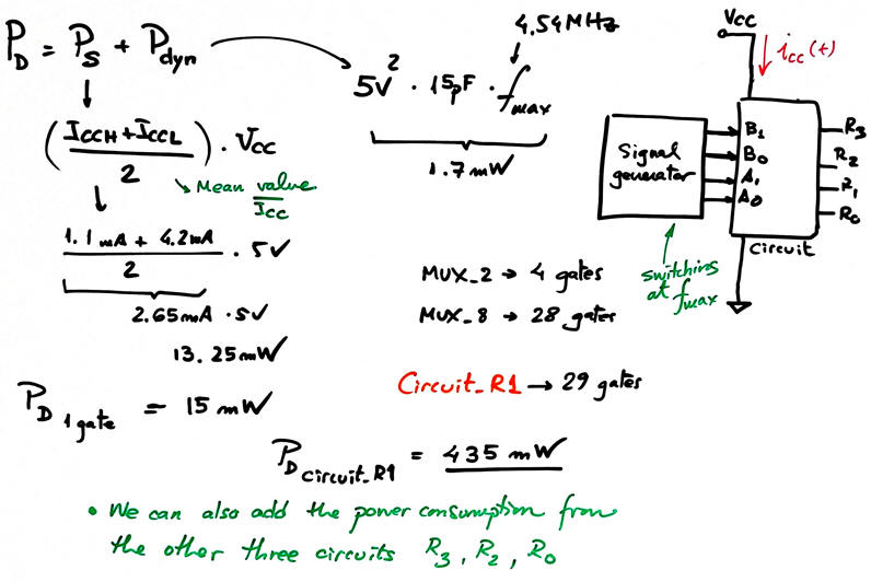
The circuit power consumption may be broadly estimated considering all the gates switching at maximum speed, thus applying the power formula for one gate to all of them. For R1 circuit,
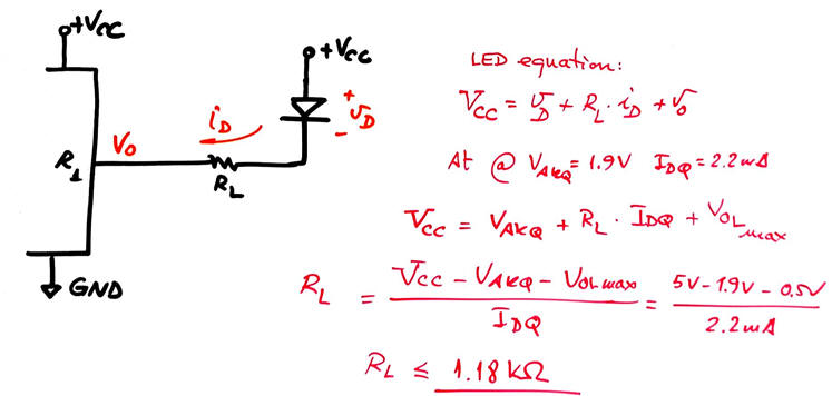
6. The LED limiting resistor RLL considering an active-low driving circuit for the worst-case scenario: VOLmax.
Problem 2
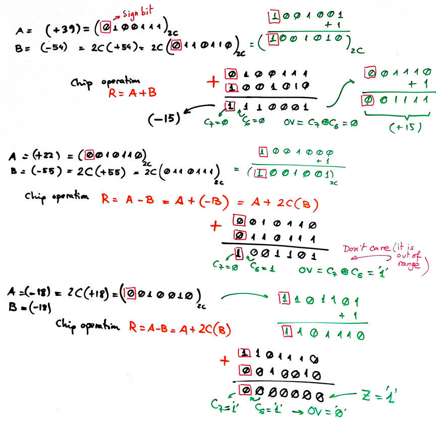
The circuit's can operate with integers from (-64) to (+63).
You can repeat the procedures in P4 for binary operations with 7-bit integers

4. The Adder_7bit component required in the top Int_add_subt_7bit can be built using ripple carry Adder_1bit components.
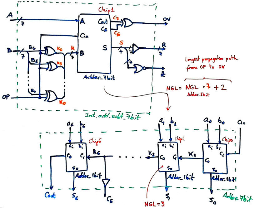
5. The longest propagation path may be inferred from input OP to output OV. Assuming that the Adder_1bit contains three levels of gates, the propagation time becomes: tP = 20 tP1g = 23· 11 ns = 253 ns. And thus the circuit's speed is 3.95 mops.
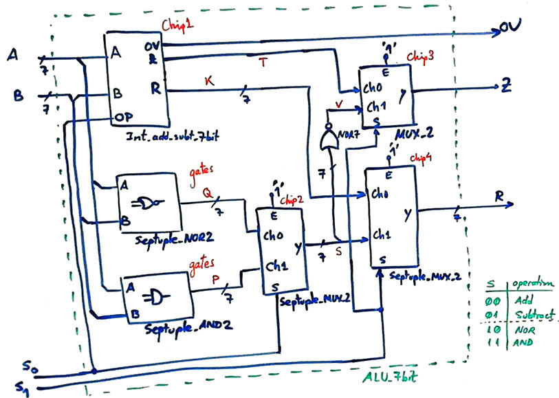
6. We can use a Septuple_MUX_2 to select between the four operations.
Problem 3
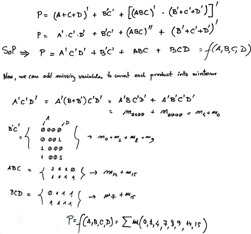
Specifications and planning concepts were studied in P1-analysis highlighted project and also in lecture L1.3. Method I consist of using algebra to simplify towards a regular SoP or PoS from the initial circuit equation. Then we can add the missing variables to generate minterms from each product or maxterms from each sum.
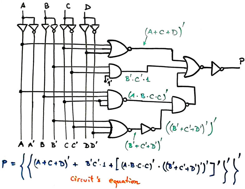
Now, we can start developing the solution simplifying the expression as follows:
You can use method II to check your solutions "Circuit_P3.pdsprj".
The analysis project using method III on circuit synthesis and functional simulation using VHDL tools is presented in LAB1.2.
Plan B strategy for capturing the circuits truth table is presented in LAB2. You can draw an schematic to adapt the truth table artefact, or instead, you can organise a flowchart.
| Home Term 26/27-Q1 Contact Products Electronic devices and companies Software Books Magazines Instruments DEE Library EETAC DEEL |

|
|
| Web activa des de 09/2001, @ F. J. Robert, Web editat amb Microsoft Expression Web 4. El contingut és un complement als materials d'estudi del curs Circuits i Sistemes Digitals disponibles al campus digital Atenea. Llicència:Reconeixement 4.0 Internacional de Creative Commons |