|
|
Bachelor's Degree in Telecommunications Systems and in Network Engineering |
|
|
|
|||||
Chapter 2 problems |
- D2.5 - |
LED lamp dimmer (FPGA-VHDL) |
|||
|
|
|||||
1. Specifications
Luminaries work with high efficiency LED lamps and the light generated can be dimmed using a control circuit. A typical bulb is 12W, 12V, E27 screw fitting. To modulate the light intensity we can use simple pushbuttons or rotary knots.
The same project designed programming a μC is in D3.5.
 |
|
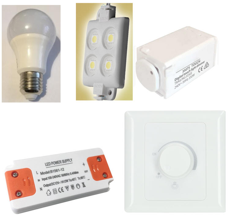
Fig. 1. Examples of luminaries, bulbs, dimmer circuits and power drivers. |
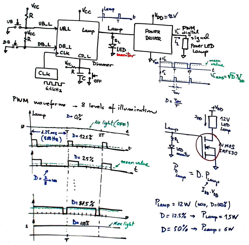
Let us propose the basic circuit for a dimmer in Fig. 2. Light intensity can be set in eight levels. Clicking button up (UB) light will increase, and clicking button down (DB) light will decrease. The idea behind controlling electrical power applied to a load like a LED bulb is to use digital pulsed width modulated waveforms (PWM). If the switching frequency is high, the eye will not be affected by flickering.
Let us invent a circuit capable of generating a 800 Hz PWM signal (T = 1.25 ms) with duty cycle modulations (D%) of 0, 12.5, 25, 37.5, 50, 62.5, 75, 87.5, 100.
 |
|
Fig. 2. Symbol and connection to a power lamp driver. |
The lamp power driver can be designed later using power MOS transistors or we can buy it along with the 5 V and 12 V power supplies. At this initial phase a simple standard LED can be used to monitor the light intensity or brightness generated at the Lamp output.
2. Planning
Better organise the design of a commercial product planning several phases.
Design phase #1: basic features.
Solve the circuit for the design step #1. Only when it is fully tested working correctly and reported, solve the design step #2.
- Design step #1. Consider an initial circuit with only the up button UB.
- Design step #2. Add the down button DB (circuit in green).
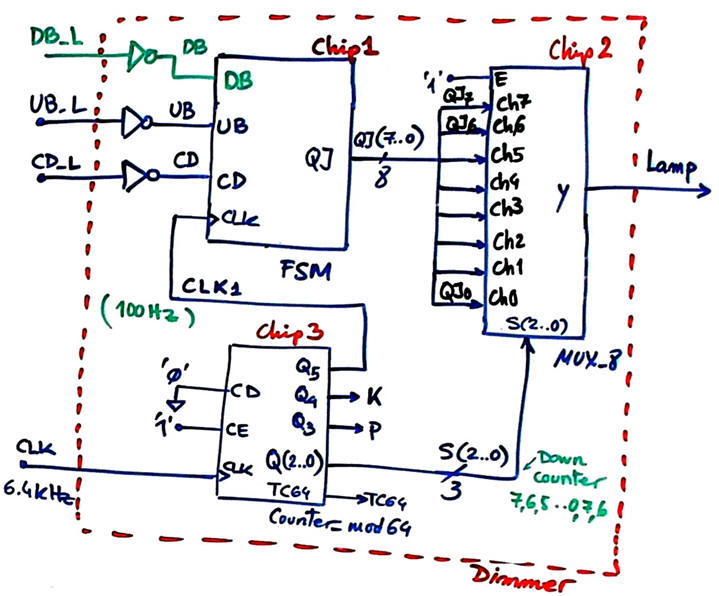
The circuit architecture is represented Fig. 3. When clicking buttons, the FSM generates adjacent 8-bit Johnson codes that are multiplexed at 6.4 kHz, thus producing a 800 Hz Lamp output signal.
A standard Counter_mod64 (P7) can be designed to generate the MUX_8 selection input and also the FSM CLK1 squared signals. Buttons are sampled at the FSM CLK frequency (TCLK = 10 ms).
 |
|
Fig. 3. Dimmer circuit architecture. |
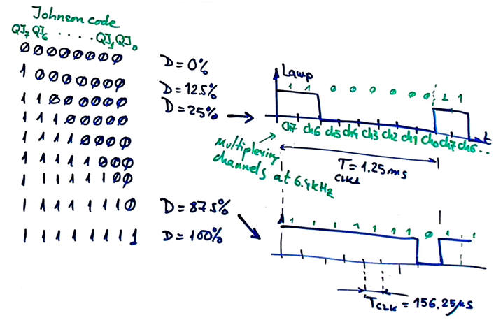
Using the MUX_8 driven from the 8-bit Johnson code we will generate the PWM waveforms in Fig. 4.
 |
|
Fig. 4. Codes required at MUX_8 input channels. |
Some questions to kick off the project and organise it step by step. Firstly we will design the FSM chip, secondly we can proceed with the top dimmer:
FSM
Draw some waveforms in a timing diagram as in Fig. 5.
 |
|
Fig. 5. Example timing diagram watching states when clicking UB several times. |
Imagine how the FSM circuit will work. Infer how many resources the circuit may contain and try to draw a state diagram for the circuit's FSM as shown in Fig. 6.
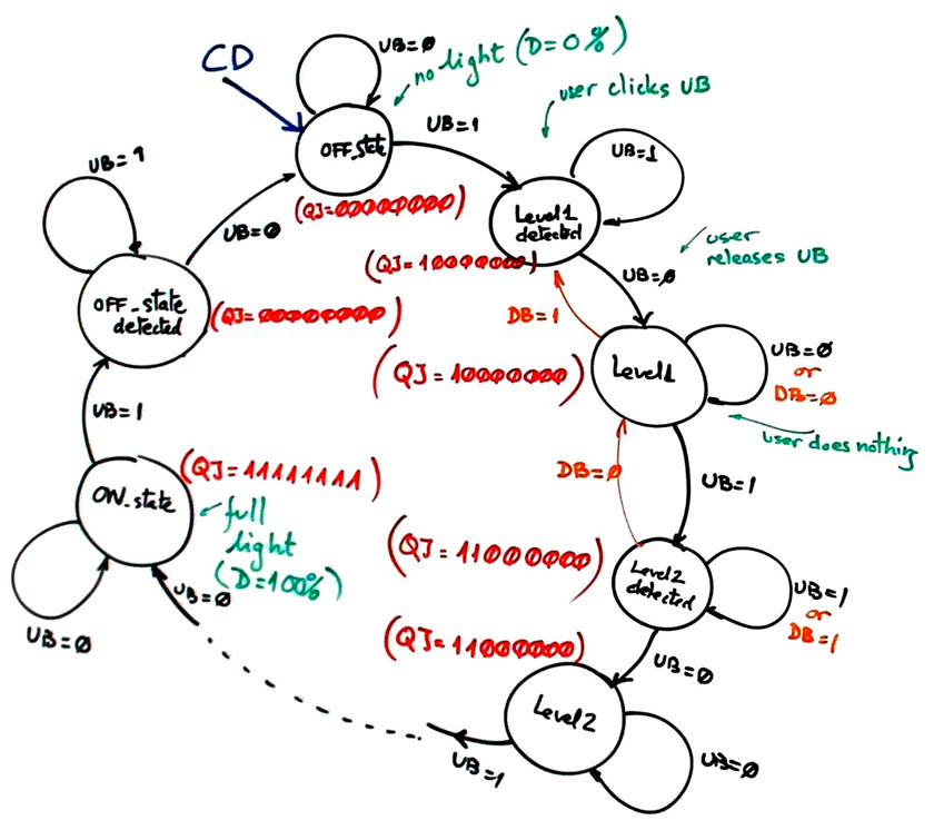 |
| Fig. 6. Example of state diagram to generate an 8-bit Johnson code and to track the button clicking. Do not consider the DB is the first design step. |
Apply the FSM architecture to this problem.
Deduce how many D_FF are required when encoding FSM states using the following options and draw the state register memory:
Option #1: radix-2 (sequential)
Option #2: Gray
Option #3: Johnson
Option #4: one-hot
Draw the state register based on D_FF considering your state encoding option.
Write the truth table of CC2 and CC1 and their equivalent behavioural interpretations (plan B) using flowcharts.
Project location:
C:\CSD\P6\dimmer\(files)
Write the FSM VHDL file.
Start a Quartus Prime synthesis project for one of the following programmable target chips:
Option #1: Cyclone IV EP4CE115F29C7
Option #2: MAX II EPM2210F324C3
Inspect and annotate the RTL and technology views. Check the number of D_FF synthesised in this application.
Dimmer
Design or adapt the other components in the top structure Dimmer and synthesise and test it. For example, Fig. 8 shows how the down Counter_mod64 used for both, generating the MUX_8 selection signals and the 100 Hz CLK1 can be inferred using standard components Counter_mod16 and logic gates (plan C2) in L7.3.
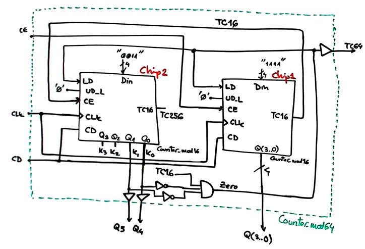 |
| Fig. 8. Inventing the Counter_mod64 expanding basic blocks Counter_mod16. |
Prepare a VHDL testbench fixture to adapt the stimulus signals in the Fig. 5 sketch. Rely on the constant CLK_Period for setting the time scale.
|
|
|
Fig. 7. Testbench fixture. What inputs, outputs and internal signals are to be monitored? |
Run functional simulations to verify your design. Visualise as well in the wave timing diagram the internal states.
Measure the propagation time CLK to output (tCO)using gate-level simulations.
What may be a good estimation of the maximum frequency of operation? Explain your answer.
Optional. Design step #3. Whatever the light intensity, if the user presses one of the two buttons more that 2 s, the light is switch off. Thus, detecting long clicks simplifies the lamp control.
Design phase #2: Additional features to enhance the product such crystal oscillator for CLK signals and presence detector for saving energy.
- Design step #1: Design a CLK generator to obtain the 6.4 kHz square wave from a 50 MHz quartz crystal oscillator like the one available in the DE10-Lite board. Deduce the number of D_FF that the Dimmer will contain.
- Design step #2: Modify the circuit adding a Timer and a presence or motion detector (PD), so that after 3.2 minutes of detecting no one in the room, the system goes to Off_state, as a way to save energy as in most modern buildings. Another interesting option is to disable the lamp on daylight when installed outdoors.
- Design step #3: Add an infrared (IR) transmitter/receiver module to operate the lamp Dimmer using a remote control as with the wall pushbuttons.
| Home Term 24/25-Q1 Contact Products Electronic devices and companies Software Books Magazines Instruments DEE Library EETAC DEEL |

|
|
| Web activa des de 09/2001, @ F. J. Robert, J. Jordana. Web editat amb Microsoft Expression Web 4. El contingut és un complement als materials d'estudi del curs Circuits i Sistemes Digitals disponibles al campus digital Atenea. Llicència:Reconeixement 4.0 Internacional de Creative Commons |