|
|
Bachelor's Degree in Telecommunications Systems and in Network Engineering |
|
|
|
|||||
Chapter 2 problems |
- D2.4 - |
Pattern detector (FPGA-VHDL) |
|||
|
|
|||||
Project version: V1 Project version: V2
1. Specifications (Version #1)
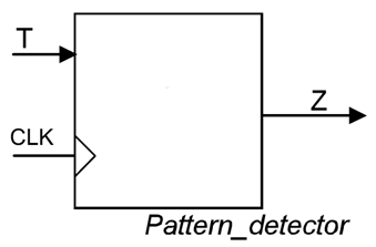
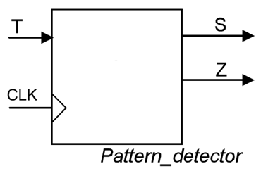
Our aim is to implement a circuit to detect a given binary pattern received from a radio or wired transmitter bit stream at input T. Fig. 1 shows the symbol of this pattern_detector circuit.
The same project designed programming a μC is in D3.4.
The detected pattern is an option, for instance:
-Option #1: "0110"
-Option #2: "11010" (use the option given by your instructor)
The remaining indications in this page are adapted to the pattern in option #1.
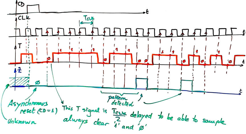
When the sequence "0110" is detected, output Z goes high for one CLK period. Two or more adjacent patterns can also be detected as in this bit stream sequence: "01101101101..."
To make te design simpler than the D2.5 version, we will assume:
- The bitstream incoming frequency is the same of the pattern_detector CLK.
- The bit stream signal is delayed half period (180°) with respect the CLK, to be able to sample stable data on the CLK rising edges.
- The detector is working continuously once the power supply is turned on.
 |
|
Fig. 1. Symbol. |
The best way to start, is to try imagining how the output will be for a given bitstream, as represented in Fig. 2.
 |
|
Fig. 2. Example of timing diagram. |
NOTE: The idea is to read and study as much as you like materials, books, examples or advanced tutorials, but do not copy from them. pattern detectors are used as project examples in most of the reference books. Your aim is to imagine that this project is derived from the LAB6 tutorial where we organised a FSM controlled clicking a single button. The better you comprehend the laboratory tutorial the faster will you design this application.
2. Planning ideas
The planning is based on applying our FSM recipe. This architecture is translated to VHDL as a plan C1 single file where the three main components are processes.
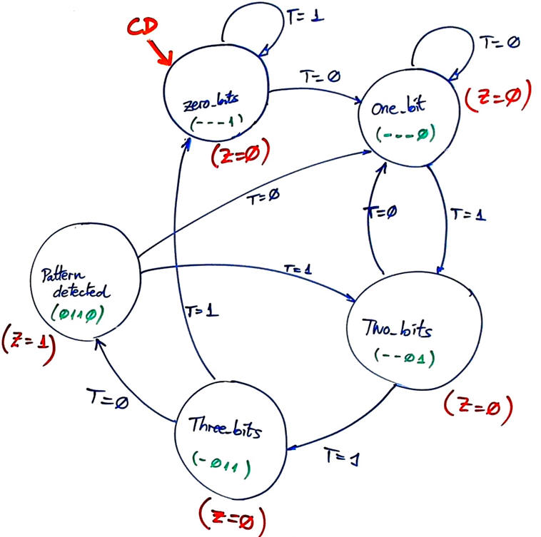
Draw a state diagram for the circuit's FSM. Fig. 4 shows an example, however you may imagine a different one.
 |
|
Fig. 4. Example of state diagram. States in this application represent the "memory", this is how many bits of the pattern sequence are known at a given time. Five states are required, and we will assume that a CD pulse inicialises the circuit to the state zero_bits where not a single bit of the pattern is yet known. |
Adapt the FSM architecture to this problem, naming and connecting all signals and inputs and outputs.
Deduce how many D_FF are required when encoding FSM states using the following options and draw the state register memory:
Option #1: radix-2 (sequential)
Option #2: Gray
Option #3: Johnson
Option #4: one-hot
Draw the FSM state register memory block.
Write the truth table of CC2 and CC1 and their equivalent behavioural interpretations (plan B) using flowcharts.
Project location:
C:\CSD\P6\pattern\(files)
Write the FSM VHDL file.
Start a Quartus Prime synthesis project for one of the following programmable target chips:
Option #1: Cyclone IV EP4CE115F29C7
Option #2: MAX II EPM2210F324C3
Inspect and annotate the RTL and technology views. Check the number of D_FF synthesised in this application.
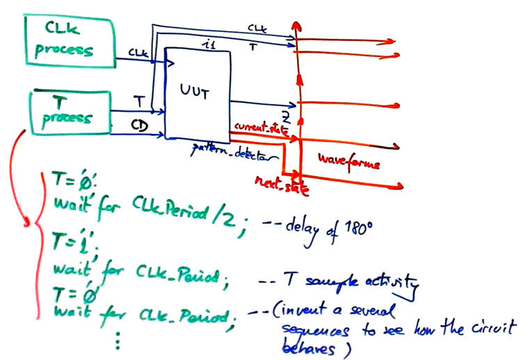
Generate a VHDL testbench fixture schematic.
Prepare a VHDL testbench fixture to adapt the stimulus signals in the Fig. 2 sketch. To translate such waveforms into a testbench process for driving T, it is necessary to rely on the constant CLK_Period for both, generating the initial delay and implementing the bit sequence.
 |
|
Fig. 3. Example of the T process generation. |
Run functional simulations to verify your design. Visualise as well in the wave timing diagram the internal states.
Run gate-level simulations to measure the propagation time CLK to output (tCO). Measure the minimum TCLK period or the maximum frequency of operation of the FSM.
Optional: how can such circuit, using another design phase, be made programmable? What kind of new hardware will be involved to detect several patterns?
Optional: If such circuit has to be prototyped and characterised in the lab, how can we invent an intrument such a programmable pattern generator to be the source of the bit stream for testing and verifying our detector D2.22?
|
|
|||||
Chapter 2 problems |
- D2.4 - |
Designing a pattern detector (FSM). |
|||
|
|
|||||
1. Specifications (Version #2)
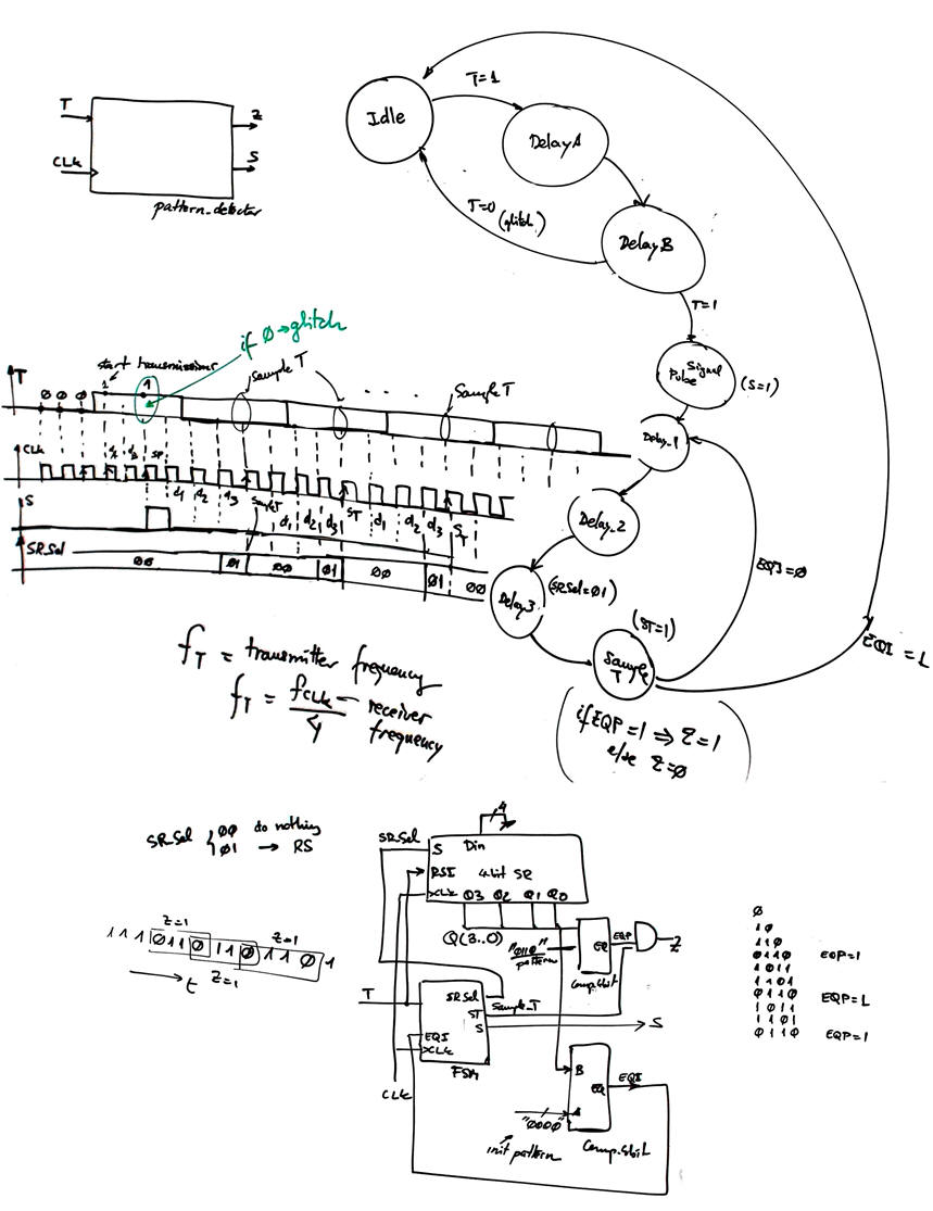
Our aim is to implement a circuit to detect the binary pattern "0110" received from a radio transmitter bit stream at input T. The symbol of which is represented in Fig. 1.
In order to adjust sampling time in the middle of each transmitted bit, the receiver CLK frequency is four times the transmitter frequency.
When there is no transmission, the receiver is sampling '0' and is kept idle.
When the first '1' is detected, output S goes high for one CLK as a flag to indicate that transmissions are starting. The receiver delays two CLK periods and if the value sampled is yet '1', it starts sampling continuously every four CLK periods. This synchronisation mechanism means that the receiver will sample input T values when signal is stable aproximately at half of the transmission period, far away from T signal transitions.
When the pattern "0110" is detected output Z goes high for one CLK period. Two or more adjacent patterns can also be detected as in this bit stream sequence: "01101101101.."
When four '0' are detected consecutively (pattern "0000"), the transmitter has stopped emitting or something went wrong with the bit stream and thus, the receiver must go back to idle.
 |
|
Fig. 1. Symbol. |
Some questions to kick off the project and organise it in four phases:
a) Infer how many resources the circuit may contain and try to draw a state diagram for the circuit's FSM. Fig. 2 shows preliminary draft ideas and discussion on how the circuit may be organised. Can a FSM block do all the work, or in this application other components such comparators and memory devices (shift registers for instance) are also necessary?
 |
|
Fig. 2. Initial discussion on the blocks and states that may be involved in our pattern detector. |
b) Apply the FSM architecture to this problem and draw the state register based on D_FF. Deduce how many D_FF are required if coding states in binary sequential (radix-2).
c) Write the truth table of CC1 and CC2 and their equivalent behavioural interpretations using flowcharts.
d) Write the FSM VHDL file and connect all the other components in the top structure. Develop the circuit for a MAX II target chip using EDA tools. Inspect the RTL and technology views. How many D_FF registers are used in this application?
e) What is the maximum transmitter CLK if an Intel MAX II CPLD is used as the target chip to implement the prototype?
| Home Term 24/25-Q1 Contact Products Electronic devices and companies Software Books Magazines Instruments DEE Library EETAC DEEL |

|
|
| Web activa des de 09/2001, @ F. J. Robert, J. Jordana. Web editat amb Microsoft Expression Web 4. El contingut és un complement als materials d'estudi del curs Circuits i Sistemes Digitals disponibles al campus digital Atenea. Llicència:Reconeixement 4.0 Internacional de Creative Commons |