|
|
Bachelor's Degree in Telecommunications Systems and in Network Engineering |
|
|
|
|||||
Chapter 1 problems |
- D1.18 - |
12-bit arithmetic & logic unit (ALU) |
|||
|
|
|||||
1. Specifications
We aim to copy some of the 32 operations performed by the classic 74LS181 chip extending the arithmetic and logic unit (ALU) capacity to n = 12 bit. Let us use plan C2. Fig. 1 shows the 16 logic and arithmetic operations to be implemented. The idea is to synthesise this entity ALU_12bit in an target FPGA to be used as a convenient building block in signal processing applications. This Proteus circuit ALU_74LS181.pdsprj shows how this classic chip operates in 4-bit.
The same project B3.18 is proposed in Chapter 3 for learning the basics of μC software organisation and basic digital I/O.
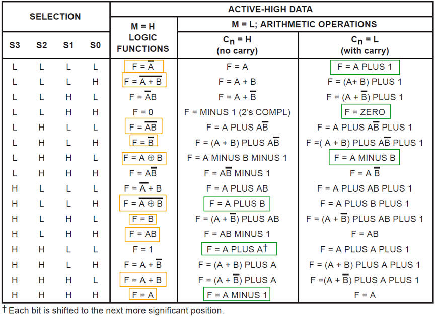 |
Fig. 1. Example operations from chip 74LS181, a 4-bit ALU in LS-TTL technology. |
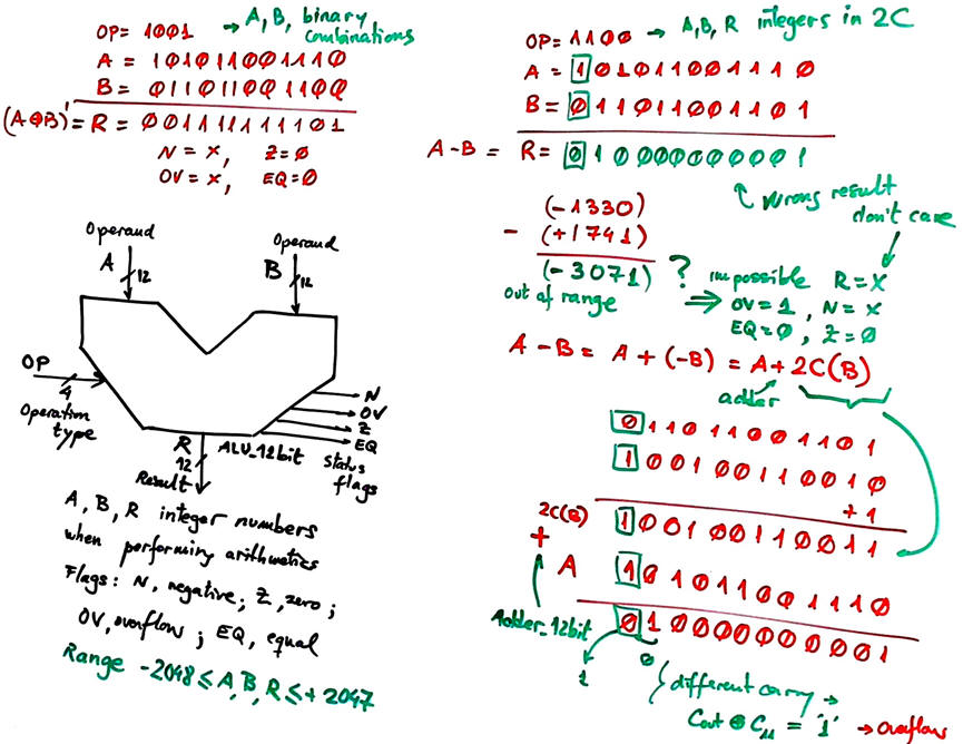
The circuit symbol and a couple of operations are represented in Fig. 2. Observe the range of the integer numbers A, B and result R when working in arithmetic mode.
 |
|
Fig. 2. ALU truth table and operations. |
The full truth table representing ten bitwise logic operations and six 2C integer arithmetic operations is shown in Fig. 3.
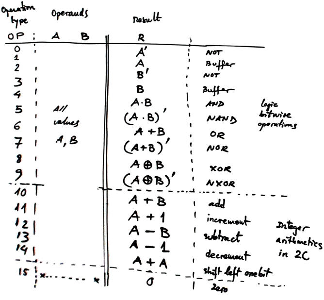 |
Fig. 3. ALU_12bit truth table. |
Draw an example of timing diagram to be used later as stimulus in the VHDL testbench when verifying the synthesised circuit. Consider Min_Pulse = 2.78 ms.
Example of test options for checking the project, try at least these numbers and operations and check also status flag values:
Option #1: Operations OP: 3, 6, 9, 10, 12, 14, 15, try some integers A, B: (-203), (+1045), (-2010),(-2048), etc.
Option #2: Operations OP: 1, 3, 8, 10, 12, 13, 15; try some integers A, B: (-508), (+1945), (-2044), (-2048), etc.
Option #3: Operations OP: 0, 2, 4, 7, 10, 12, 11, 15; try some integers A, B: (-667), (+1894), (-2032), (-2048), etc.
2. Planning
Some ideas on planning. Draw the general architecture of the ALU_12bit as shown in Fig. 4. Imagine several design steps and infer the type of basic components required. How can you optimise such circuit? This is what we will propose here, instead of designing the general architecture in Fig. 4, we can combine several similar operations and reduce the size of the multiplexers and the arithmetic operators.
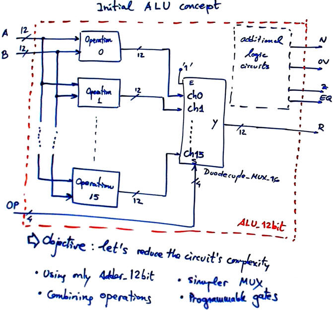 |
Fig. 4. ALU general architecture is a large circuit capable of operating 256M combinations. |
Observing the circuits truth table, we can reduce the circuit complexity, for instance using a single Adder_12bit for all the arithmetic operations and using XOR gates as NOT or buffers. Study in detail the lecture L4.2 and also the P4 highlighted circuit on 2C integer arithmetic.
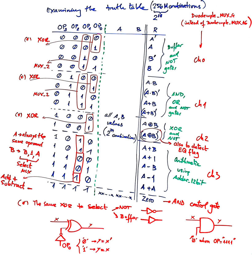 |
Fig. 5. Ideas to reduce the circuits complexity. XOR gates can be used as programmable gates: acting as a NOT or as a buffer. OP inputs can be used to select operands. |
Thus, Duodecuple_MUX_2 can be used to select operators and obtain a much simpler circuit. We can solve firstly the bitwise logic operations. And group the arithmetic operations in a single block, as shown in Fig. 6.
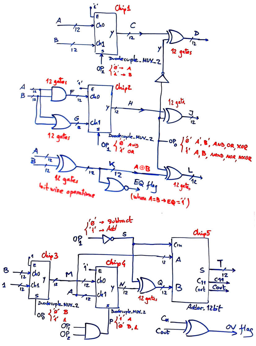 |
Fig. 6. Logic and arithmetic subcircuits. The key component is the Duodecuple_MUX_2. |
Now, we can reduce the size of the final multiplexer to be a Duodecuple_MUX_4 with extra logic for its selection inputs. The result from all five arithmetic operations, signal vector T(11..0), is Ch3., as shown in Fig. 7.
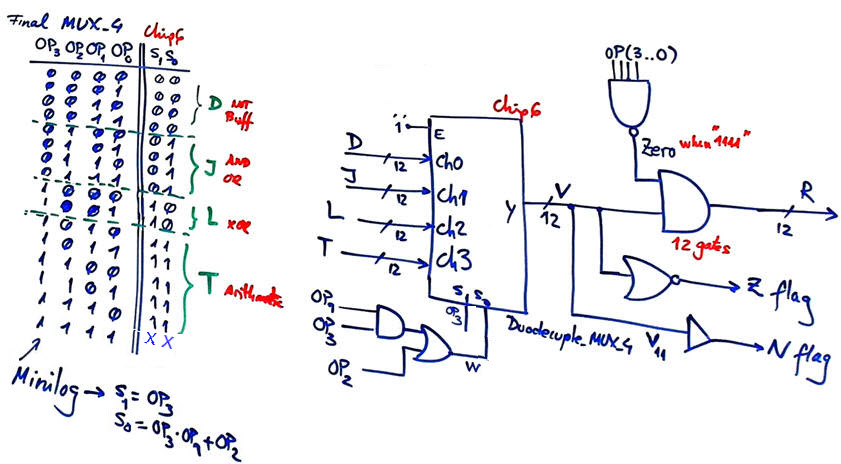 |
Fig. 7. Final Duodecuple_MUX_4 and remaining flags N, OV and Z. |
Analyse the circuits proposed, try to see how the circuit multiplexers select operands and how the result is calculated. Additional components and chips can be found and adapted from our project list.
KEY NOTE: Be aware that you have to develop this circuit step by step starting with only a few components or operations and running all the developing and testing FPGA design flow. Start drawing Fig. 6 and Fig 7 in a single sheet to see better the complete architecture of the ALU_12bit.
For example:
Step #1: Specify, plan, develop and test in your portable computer an Adder_12bit. Find similar components and and strategies from other projects. In this way you get a good training in plan C2 focusing all your attention in a single component. Do not develop (translate into VHDL) until your plan is completely annotated. Use the option indicated below (RC or CLA) for your Adder_12bit. This project will be reported as an annex.
Step #2: Invent the Duodecuple_MUX_2 adapting the Dual_MUX_4 plan B, because a behavioural flowchart is much simpler that using equations. This project will be reported as an annex.
Step #3: Translate the ALU_12bit schematic into VHDL and develop and test the project using the numbers and values given in your option. This task will become the main report.
The key component in this design is the Adder_12bit. It can be internally conceived using two strategies:
Adder option #1: Ripple carry (RC) as shown in a similar circuit in LAB3. You can use smaller adders and chain them ripplying carry signals.
Project location:
C:\CSD\P3\ALU_12bit\RC\(files)
Adder option #2: Carry-lookahead (CLA). You can chain three Adder_4bit or adapt this Adder_16bit.
Project location:
C:\CSD\P3\ALU_12bit\CLA\(files)
3. Development
Circuit synthesis. CPLD or FPGA target chip options:
Target option #1: MAX II
Target option #2: Cyclone IV
Target option #3: MAX 10
How many FPGA resources (logic cells, logic elements, etc.) are used? What is the percentage of the target chip used in this design?
4. Test (functional)
Functional simulation using VHDL testbench. You can use at least the initial vectors given as option for your timing diagram.
After having studied P4 lectures and LAB4 tutorials, the project can continue adding the fifth section on time measurements.
5. Test (gate-level)
Perform gate-level (timed) simulations for the given target chip, you can use the same testbench fixture from the previous functional simulation. Run the timing analyser instrument.
Additional questions can be added to our report. For instance:
-
Perform a gate-level simulation to measure propagation delays in a given signal transition.
-
Deduce the worst-case propagation delay running the timing analiser tool and calculate the circuit's maximum frequency of operation for the target chip used in the design.
-
In the end, because two alternative internal circuit architectures are proposed (option #2:CLA, option #1: RC, we can compare which one is faster and which one uses less resources (logic elements).
-
And also, for each circuit architecture, because we are proposing several target chips, you can measure which technology is faster. Unfortunately, the family MAX10 does not generate the required standard delay files (-sdo) for running gate-level simulations.
Target option #1: MAX II
Target option #2: Cyclone IV
If we automate the testbench process, how long does it take to complete the full test of ths circuit if Min_Pulse = 100 ns?
Can you imagine how to enlarge such circuit to an ALU_64bit av available in each one of your portable computer cores?
| Home Term 24/25-Q1 Contact Products Electronic devices and companies Software Books Magazines Instruments DEE Library EETAC DEEL |

|
|
| Web activa des de 09/2001, @ F. J. Robert, J. Jordana. Web editat amb Microsoft Expression Web 4. El contingut és un complement als materials d'estudi del curs Circuits i Sistemes Digitals disponibles al campus digital Atenea. Llicència:Reconeixement 4.0 Internacional de Creative Commons |