|
|
Bachelor's Degree in Telecommunications Systems and in Network Engineering |
|
|
|
|||||
Chapter 1 problems |
- D1.17 - |
2-digit BCD adder |
|||
|
|
|||||
1. Specifications
Invent a 2-digit BCD adder using plan C2. When the operands tens or units inputs are invalid BCD numbers, the output is zeroed and Error = '1'.
The same project B3.17 is proposed in Chapter 3 for learning the basics of μC software organisation and basic digital I/O.
 |
|
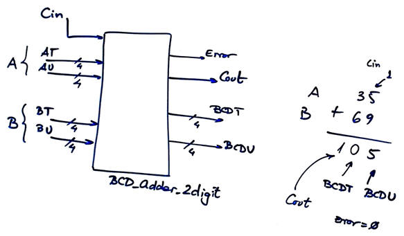
Fig. 1a. Symbol of the 2-digit BCD adder circuit and an example of operation. |
The circuit truth table signals are ordered as shown in Fig. 1b.
|
Fig. 1b. Input and output order in the truth table. |
What is the range of operands and results? You can consider several options for the test vectors including Cin = '0' and Cin = '1', such:
option #1: Numbers 67, 32, 0, 17, 99, 7
option #2: Numbers 33, 55, 87, 14, 0, 2
option #3: Numbers 38, 79, 99, 0, 17, 66
Experiment with several input vectors and calculate the outputs. Draw the truth table. How long is it?
Draw an example of timing diagram to be used later as stimulus in the testbench when verifying the synthesised circuit. Consider Min_Pulse = 1.12 μs. How long does it take to simultate all the truth table combinations?
CPLD or FPGA target chip options:
option #1: MAX II
option #2: MAX 10
option #3: Cyclone IV
2. Plan
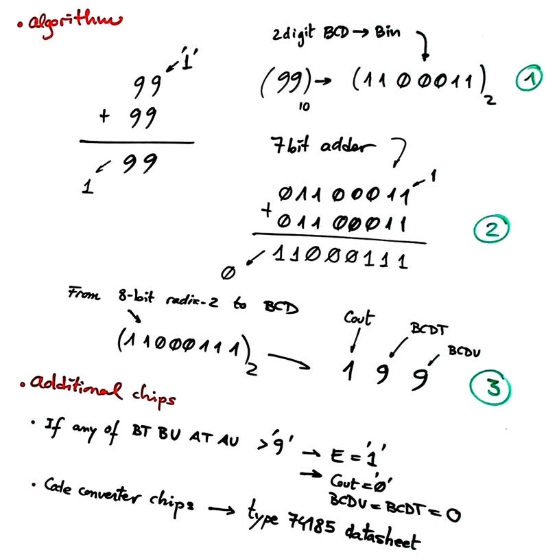
Study how the algorithm of addign digits in BCD works. Find comercial chips, even if they are obsolete, you can find good ideas to apply in your designs.
Plan C2. Draw a hierarchical circuit based on components and signals and prepare it ready for translation to VHDL.
Let us consider these options:
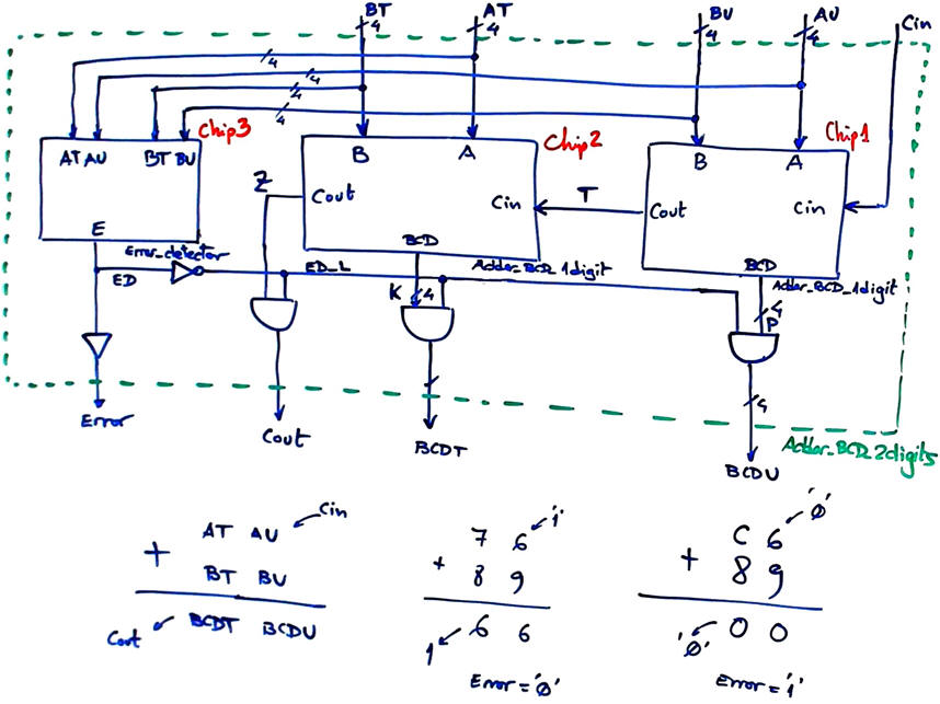
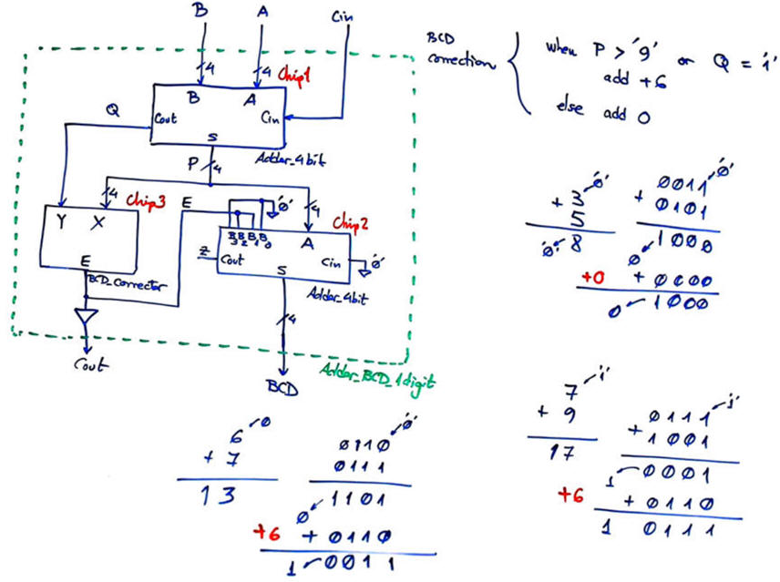
option #1: rippling or chaining 1-digit BCD adder components. Invent the component BCD_adder_1digit using Adder_1bit and other circuits.
 |
|
Fig. 2. Proposed top block diagram for the Adder_BCD_2digit in this option #1. |
 |
|
Fig. 3. Proposed internal design for the circuit Adder_BCD_1digit component. |
Project location:
C:\CSD\P3\BCD_adder_2digit\Opt1\(files)
Design steps. To make the design simpler and easy to debug and also for obtaining parcial marks, we usually organise several steps. For instance,
- step #1: leave the Error_Detector circuit architecture empty, containing only E <= '0';
- step #2: add the internal architecture and circuits to detect when an input operand is invalid.
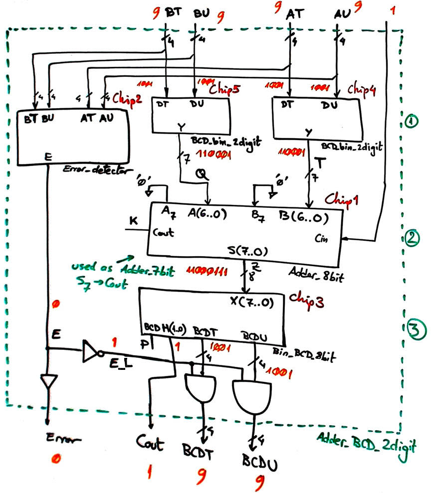
option #2: using an Adder_7bit and BCD-to-binary and binary-to-BCD code converters.
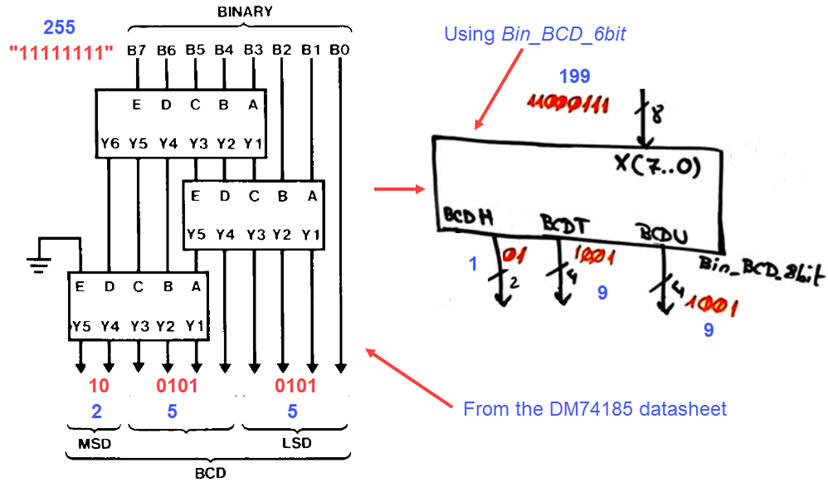
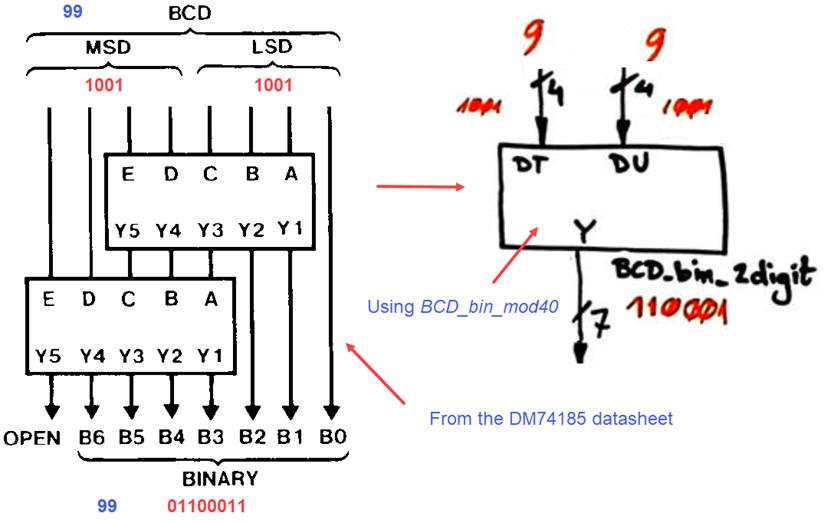
The 74184/185 datasheet shows the basic components BCD to binary radix-2 modulo 40 converter (DM74184) and olso the basic 6-bit binary radix-2 to BCD converter (DM185). The idea is that the basic DM74185 expandable block can be adapted and solved in a flat single VHDL file using plan B (copying truth tables) Bin_BCD_6bit or plan A (minimising equations) Bin_BCD_6bit. And in the same way, the DM184 can be adapted using plan B as shown in the tutorial BCD_bin_mod40 example.
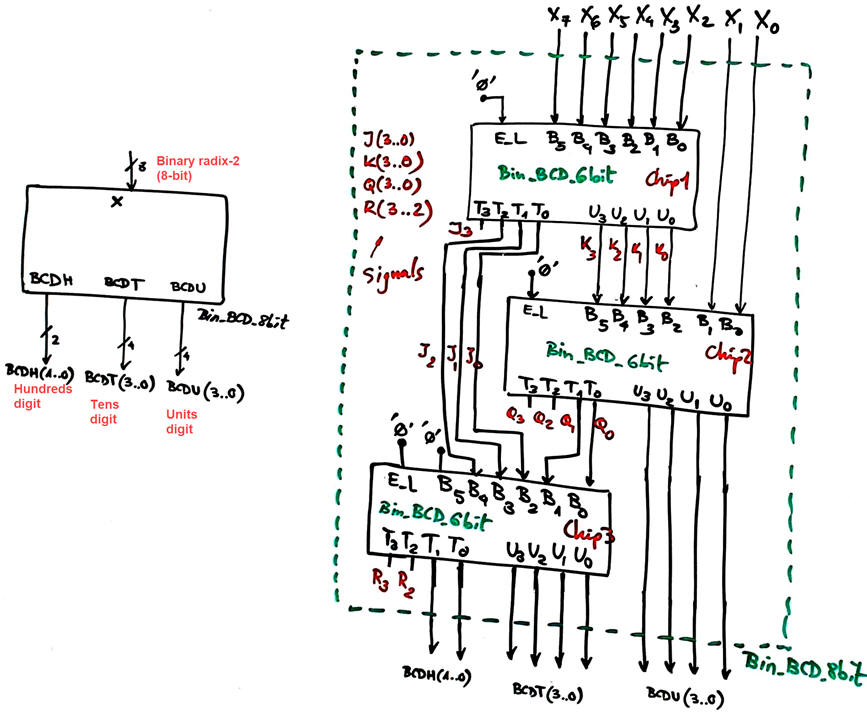
And, in the same datasheet, we learn how to expand converters to a larger number of bits or digits. More ideas can be found in assignments D1.15 and D1.16. In this project a BCD_bin_2digit and a Bin_BCD_8bit chips will be required.
  |
|
Fig. 4. Proposed top block diagram for the Adder_BCD_2digit in this option #2. The operation shown is truth table maximum computable value. Input operands above '9' will generate error. |
Project location:
C:\CSD\P3\BCD_adder_2digit\Opt2\(files)
Design steps. To make the design simpler and easy to debug and also for obtaining parcial marks, we usually organise several steps. Think how to grow this circuit so that you can complete the full schematic in several steps.
Using Fig. 5 ideas generate the schematic for the component Bin_BCD_8bit ready for VHDL translation.
  |
|
Fig. 5. In the datasheet we find information on how to expand several bin-to-BCD converter (Bin_BCD_6bit) to obtain our Chip3 Bin_BCD_8bit. |
Using Fig. 6 ideas generate the component BCD_bin_2digit ready for VHDL translation.
 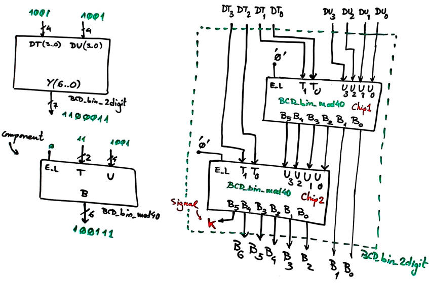 |
|
Fig. 6. In the datasheet we find information on how to expand several BCD-to-binary radix-2 converter (BCD_bin_mod40) to obtain our Chip4 and Chip5 BCD_bin_2digit. |
3. Development
Circuit synthesis
4. Test (functional)
Functional simulation
After having studied P4 lectures and LAB4 tutorials, the project can continue adding the fifth section.
5. Test (gate-level)
Additional questions can be added to our report. For instance:
-
Perform a gate-level simulation to measure propagation delays in a given signal transition.
-
Deduce the worst-case propagation delay running the timing analiser tool and calculate the circuit's maximum frequency of operation for the target chip used in the design.
-
In the end, because two alternative circuits are proposed (option 1 and option 2), we can compare which one is faster and which one uses less resources (logic elements).
| Home Term 24/25-Q1 Contact Products Electronic devices and companies Software Books Magazines Instruments DEE Library EETAC DEEL |

|
|
| Web activa des de 09/2001, @ F. J. Robert, J. Jordana. Web editat amb Microsoft Expression Web 4. El contingut és un complement als materials d'estudi del curs Circuits i Sistemes Digitals disponibles al campus digital Atenea. Llicència:Reconeixement 4.0 Internacional de Creative Commons |