|
|
Bachelor's Degree in Telecommunications Systems and in Network Engineering |
|
|
|
Adder_16bit plan C2: ripple-carry (RC) |
16-bit adder for radix-2 numbers
| 1. Specifications | Planning | Developing | Functional test | Gate-level test | Prototype | Report |
Design an Adder_16bit using the ripple-carry technique (RC).
The truth table and timing diagram are the same stated in Adder_4bit RC considering now radix-2 operands A and B ranging from 0 up to 65535 = "1111 1111 1111 1111".
 |
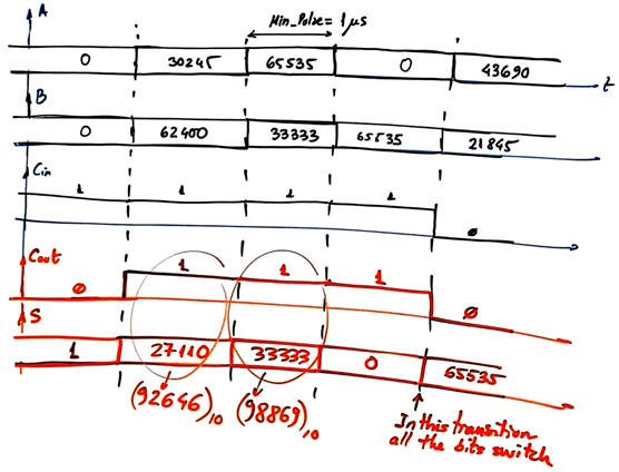 |
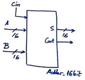
| Fig. 1. Symbol and example waveforms and operations. |
|
Here we rely on the work done when designing the tutorial Adder_4bit ripple-carry (RC). Zero (Z) flag will not be implemented, it simply adds another level of gates and is not necessary for the purpose of comparing with the Adder_16bit CLA presented below as the third project in this lab session.
| Specifications | 2. Planning | Developing | Functional test | Gate-level test | Prototype | Report |
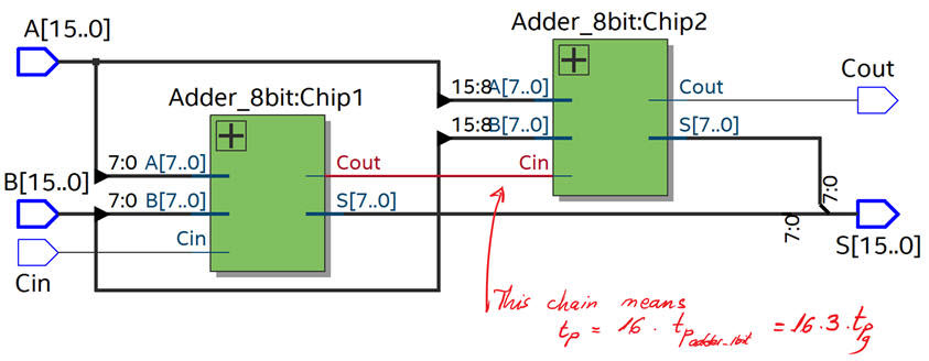
Fig. 2 shows the ripple-carry architecture. Remember that we already have designed Adder_8bit component in LAB 3 using the same carry chain strategy.
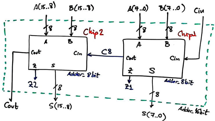 |
| Fig. 2. Adder_16bit architecture proposed chaining two components Adder_8bit. |
What is the number of gate levels (NGL) expected in this circuit?
Project location:
C:\CSD\P4\Adder_16bit_RC\(files)
| Specifications | Planning | 3. Developing | Functional test | Gate-level test | Prototype | Report |
Let us pick up a MAX II EPM2210F324C3 target chip.
VHDL file translation of the architecture in Fig. 2: Adder_16bit.vhd.
Components files: Adder_8bit.vhd , Adder_4bit.vhd and Adder_1bit.vhd (plan A or plan B) can be found in LAB 3.
  |
| Fig. 3. RTL view and all the files requires in this design. We suppose that the Adder_1bit is solved using equations SoP or PoS or canonical product of maxterms or sum of minterms in NGL = 3 (three gate levels). |
Technology view and project summary shows that only 32 logic elements are used for synthesising this project, saving much hardware with respect the CLA implementation Adder_16bit.
 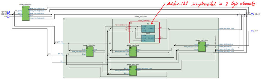 |
| Fig. 4.Technology view. Each Adder_1bit is implemented in two logic elements. To make it simple and comparable to classic technologies, we can imagine that the Adder_1bit is solved using NGL = 3. |
| Specifications | Planning | Developing | 4. Functional test | Gate-level test | Prototype | Report |
This is the translation of the testbench fixture and some signal activity proposed in Fig. 1: Adder_16bit_tb.vhd. It can be used for both, functional and gate-level simulations. Remember as well that this testbench fixture will be the same for the next project Adder_16bit based on the CLA architecture.
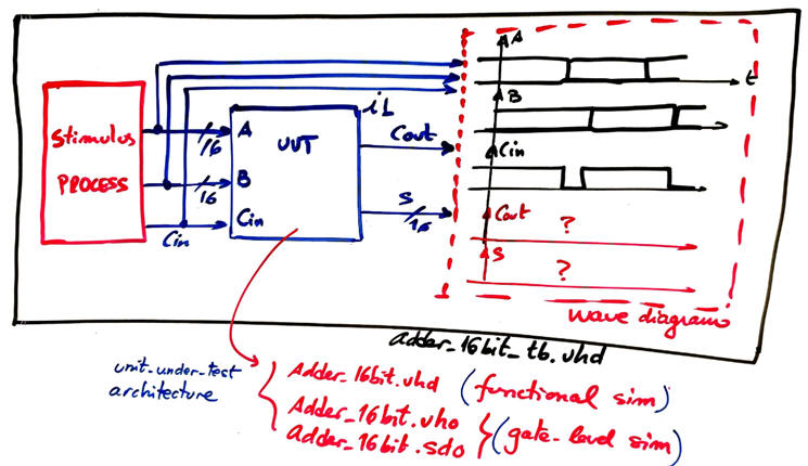 |
| Fig. 5. VHDL testbench fixture. The UUT is described as a hierarchical VHDL project when performing a functional simulation, and as a flat technology circuit when solving the gate-level simulation. |
KEY idea: the ideal functional results in this design step #4 must be identical for both project options of the same entity: ripple-carry and carry-lookahead Adder_16bit.
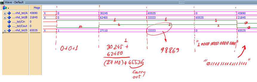 |
| Fig. 6. Functional simulation results. We simply demonstrate that this design is capable of executing the entity's truth table. |
| Specifications | Planning | Developing | Functional test | 5. Gate-level test | Prototype | Report |
Running a gate-level simulation for this ripple-carry Adder_16bit, for instance at the transition highlighted in Fig.1 where all bits have to switch, we obtain an accumulated propagation delay of tP = 22.6 ns, practically doubling the delay time produced by the CLA adder in the alternative project Adder_16bit.
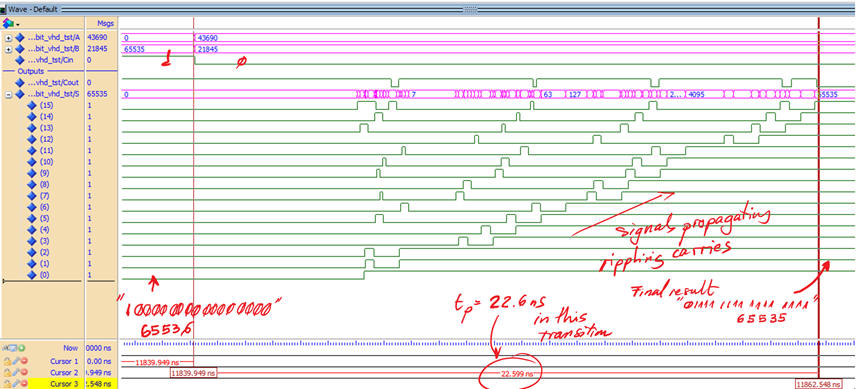 |
| Fig. 7. Gate-level simulation results at a particular transition. |
When running the timing analyser, the maximum delay occurs when driving A(0) and waiting results at Cout. This is tP= 22.7 ns, allowing a theoretical maximum operational frequency of 44 Mops (unsigned radix-2 16-bit millions of additions per second).
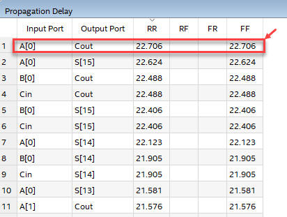 |
| Fig. 8. Timing analyser spreadsheet. |
KEY idea. Hence, at this point the answer to the question: which is the minimum value for Min_Pulse for experimentation in the laboratory becomes straightforward: Min_Pulse > tP. It becomes clear now that a value Min_Pulse smaller that the propagation delay of the circuit will imply that the circuit is going to be switching continuously, never being able to reach stable output digital values. We can verify these results using this set of vectors "Adder_16bit_tb.vhd" as represented in Fig. 9 (Min_Pulse = 25 ns) and Fig. 10 (Min_Pulse = 20 ns).
 |
| Fig. 9. Min_Pulse = 25 ns, practically on the limit, still operating. |
 |
| Fig. 10. Min_Pulse = 20 ns < tP. Thus, the outputs never settles to a valid result. |
It is time now to continue this laboratory session comparing results with the alternative carry-lookahead architecture proposed in the next project.
| Specifications | Planning | Developing | Functional test | Gate-level test | 6. Prototype | Report |
| Specifications | Planning | Developing | Functional test | Gate-level test | Prototype | 7. Report |
Follow this rubric for writing reports.
| Home Term 26/27-Q1 Contact Products Electronic devices and companies Software Books Magazines Instruments DEE Library EETAC DEEL |

|
|
| Web activa des de 09/2001, @ F. J. Robert, Web editat amb Microsoft Expression Web 4. El contingut és un complement als materials d'estudi del curs Circuits i Sistemes Digitals disponibles al campus digital Atenea. Llicència:Reconeixement 4.0 Internacional de Creative Commons |