|
|
Bachelor's Degree in Telecommunications Systems and in Network Engineering |
|
|
|
||
|
|
Dec_3_8: behavioural single-file VHDL (flat) plan B |
|
|
|
||
Binary decoder from 3 to 8 (type 74LS138)
1.Specifications
Design a binary decoder 3 to 8 active-high (Dec_3_8) following plan B based on the behavioural description of the truth table. Theory on decoders is introduced in L2.3.
These are the circuit's symbol, truth table, and example timing diagram.
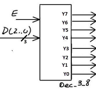
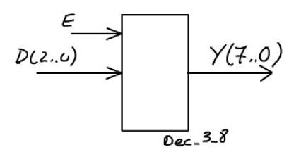 a) b) |
| Fig. 1. Dec_3_8 symbols: a) 8 independent outputs, b) vector output. |
As you can see, the symbol may be slightly different depending on the use of vector inputs.
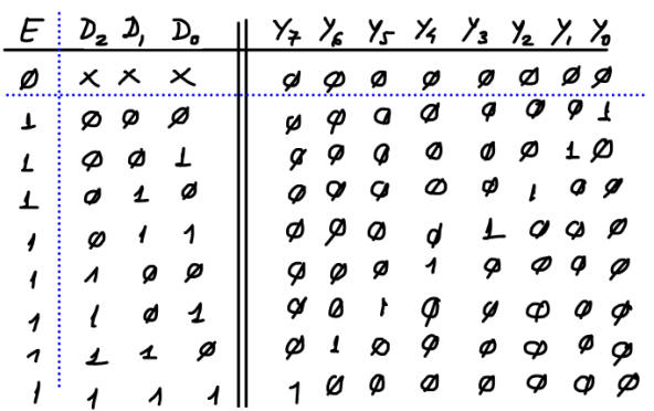 |
Fig. 2. The Dec_3_8 truth table representing active-high inputs and outputs. |
Fig. 3 shows an example of timing diagram where the Min_Pulse duration is also defined as a constant for representing time.
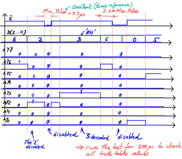 |
| Fig. 3. Example of a timing diagram showing some input activity. Later on, in design step 4, this timing diagram will be translated into a VHDL testbench as the stimulus process to run simulations. |
2. Planning
This is a mind map represesenting our VHDL design flow and the main concepts involved in designing combinational circuits.
For plan B, infer a schematic to use the truth table construct with signals and buffered input and output ports. In Fig. 4 there are the schematics for symbols a) and b) in Fig. 1.
a)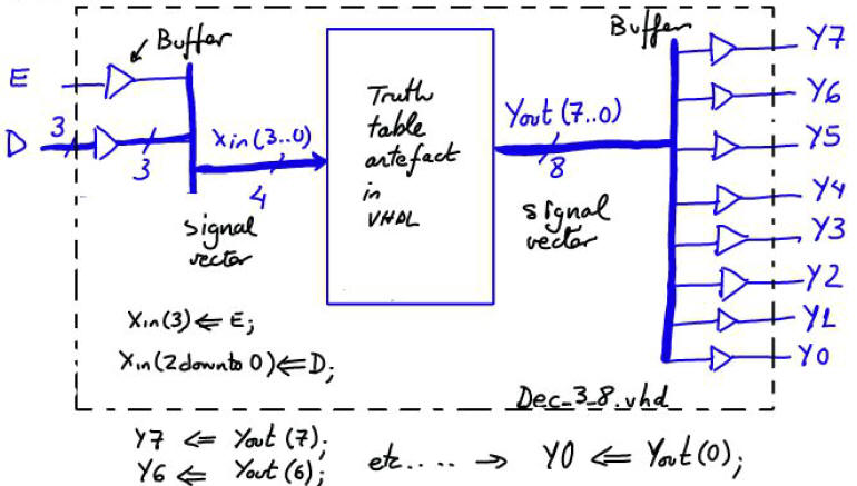 b) 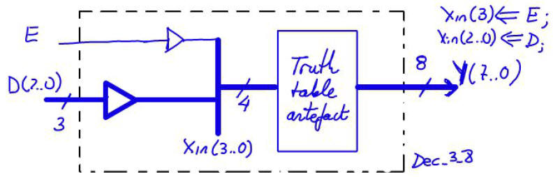 |
Fig. 4. Example schematics based on the truth table artefact for the two symbols above in Fig. 1. As you can see, when there is an vector output, the internal signal Yout(7..0) is not required. |
Another option in plan B, represented in Fig. 5, is to infer a flowchart as the interpretation of the truth table.
c)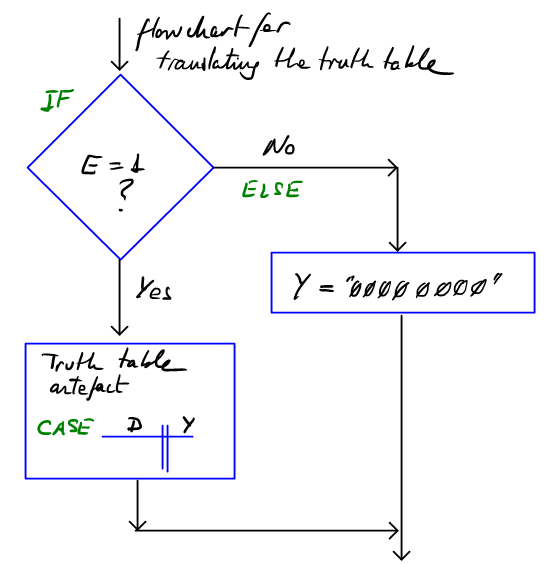 |
| Fig. 5. Version c) Interpreting the truth table as a flowchart. |
Each interpretation will generate a different VHDL file, therefore, place each plan in a different folder. For instance:
C: \CSD\P2\Dec_3_8Bc\(files)
Run a EDA tool project for a CPLD/FPGA target chip (Dec_3_8_prj).
Print RTL and technology views.
Test the project using a VHDL testbench.
3. Development
1.- Write down the VHDL file translating the schematic above in Fig. 4. This Dec_3_8.vhd is the file for the symbol a). This Dec_3_8.vhd is the file for the symbol b), and this Dec_3_8.vhd is the translation of the flowchart c).
2.- Start an EDA tool project Dec_3_8_prj for a CPLD/FPGA target chip and obtain the synthesised circuit. Represent and analyse the RTL and technology views.
3.- Examine and print a commented copy of the RTL schematic. This is an example of a RTL view of the circuit synthesised by the computer tool.
4.- Examine and print a commented copy of the technology view. This is an example of a technology view when targeting the FPGA chip Spartan-3E XC3S500E-FG320 from Xilinx.
4. Testing
1.- Start an EDA VHDL simulator project and verify the Device-Under-Test (DUT) using a VHDL simulator test bench (Dec_3_8_tb.vhd).
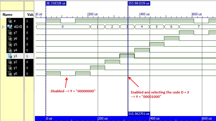
2.- Verify applying sufficient test vector that the device works as expected (verify the truth table). Print timing diagram screen and add comments on the signals to show how the device works.
This is an example of a functional simulation of the Unit Under Test (UUT).
5. Report
Project report starting with the template sheets of paper, scanned figures, file listings, docx , pptx, or any other resources
6. Prototyping
Use training boards and perform laboratory measurements to verify how the circuit works for real. The configuration file has to be downloaded into the target board as explained in the flow chart.
For example, using this pin assignment file in your project (or using the Plan Ahead tool to set the pins) you can download the configuration file to the target FPGA in the NESYS2 board and experiment with the real Dec_3_8. The driver to download the bitstream file Dec_3_8.bit is the Adept application from Digilent.
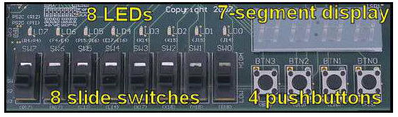 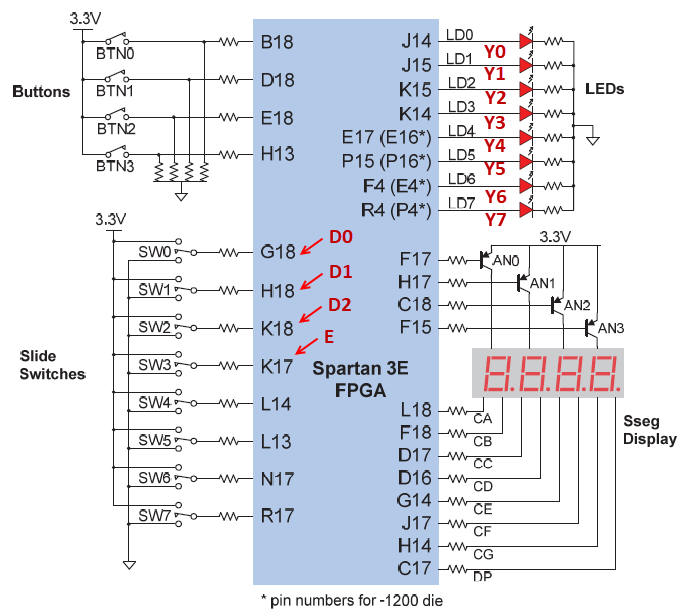 |
| Fig. 6. The LED and switch pins in the NESYS2 board. |
| Home Term 26/27-Q1 Contact Products Electronic devices and companies Software Books Magazines Instruments DEE Library EETAC DEEL |

|
|
| Web activa des de 09/2001, @ F. J. Robert, Web editat amb Microsoft Expression Web 4. El contingut és un complement als materials d'estudi del curs Circuits i Sistemes Digitals disponibles al campus digital Atenea. Llicència:Reconeixement 4.0 Internacional de Creative Commons |