|
|
Bachelor's Degree in Telecommunications Systems and in Network Engineering |
|
|
|
||
|
|
Enc_10_4 plan A: structural single-file VHDL (flat) |
|
|
|
||
Binary encoder from 10 inputs to 4 outputs (type 74LS148)
1.Specifications
Design a binary encoder 10 to 4 (Enc_10_4) with priority-high following plan A based on equations. Data inputs D_L(9..0) are active-low, enable input (Ei_L) is also active-low. Code outputs Y(3..0) are active high, and group select (GS_L) and enable output Eo_L are active low. A similar circuit is the standard Enc_8_3 74LS148.
This is some introductory theory on encoders. Mind maps that represent main concepts involved in designing combinational circuits and our VHDL design flow that allow us to observe the same entity from diverse perspectives.
These are the circuit's symbol, truth table, and example timing diagram. rec.
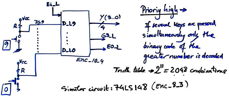 |
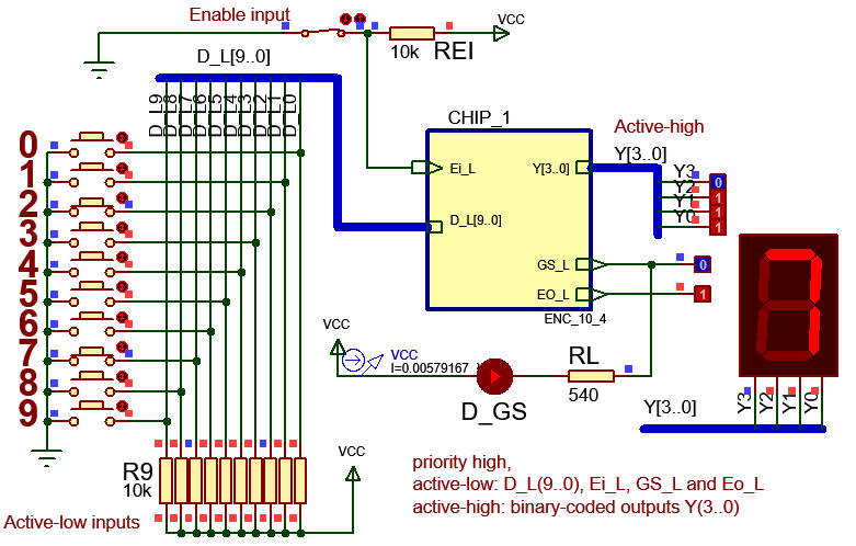
| Fig. 1. Enc_4_10 symbol and the way to connect keys as active-low or active-high. |
Fig. 2 shows how to connect active-low keys and how to drive common anode LED from an active-low chip output.
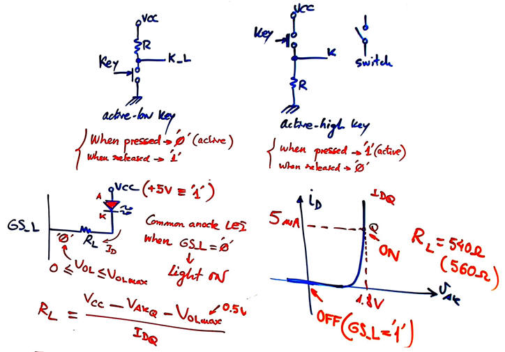 |
| Fig. 2. How to connect keys as active-low or active-high. |
Fig. 3 shows the truth table of this encoder.
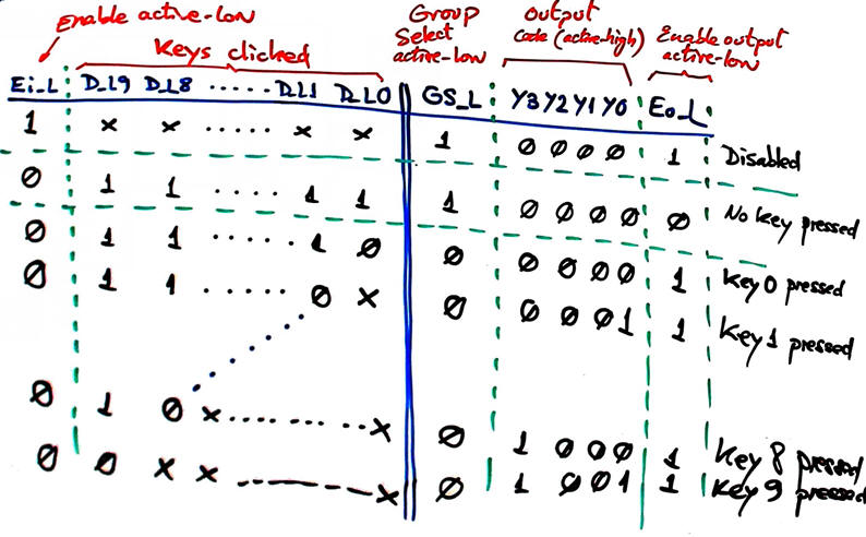 |
| Fig. 3. The Enc_4_8 truth table. |
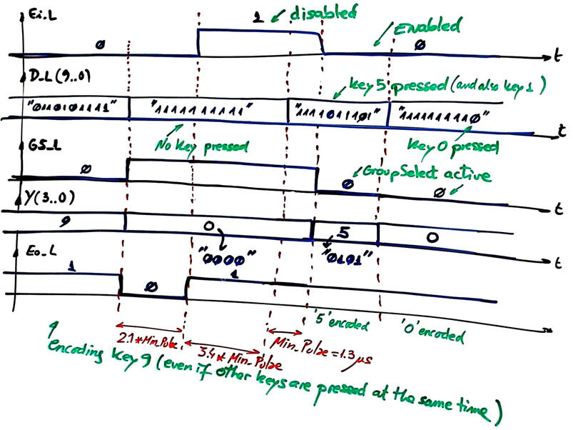
In Fig. 4 there is an example of sketch of a timing diagram. This sketch will be translated to VHDL as stimulus to drive the testbench.
 |
|
| Fig. 4. Example of a timing diagram showing some input activity and the predicted outputs for each time interval. When translating such sketch to a testbench is easy to check any output combination. | |
In Fig. 5 there is the circuit in Proteus Enc_4_10.pdsprj showing output values when clicking simultaneously key 5 and key 2 and the circuit is enabled.
 |
|
| Fig. 5. Example of circuit in Proteus. Run the simulation and comprehend how the truth table works and the meaning of input and output signals. | |
2. Planning
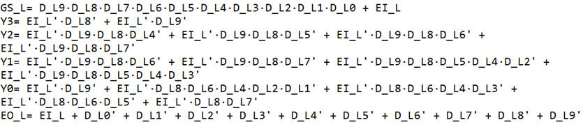
For the plan A, let us find a set of equations. Canonical minterms or maxterms are not possible because the circuit contains up to 2048 combinations. We can minimise the truth table using minilog.exe. This is the truth table as a text file Enc_4_10.tbl. Run the minimiser and obtain equations ready for translation to a VHDL architecture as in Fig. 6.
 |
|
Fig. 6. Set of equations based on SoP from minilog. Here there are also the equations in PoS. |
Project location:
C:\CSD\P2\Enc_4_10A\(files)
3. Development
1.- Write down the VHDL file translating the equations above, for instnce the set of PoS. This is an example VHDL file Enc_10_4.vhd.
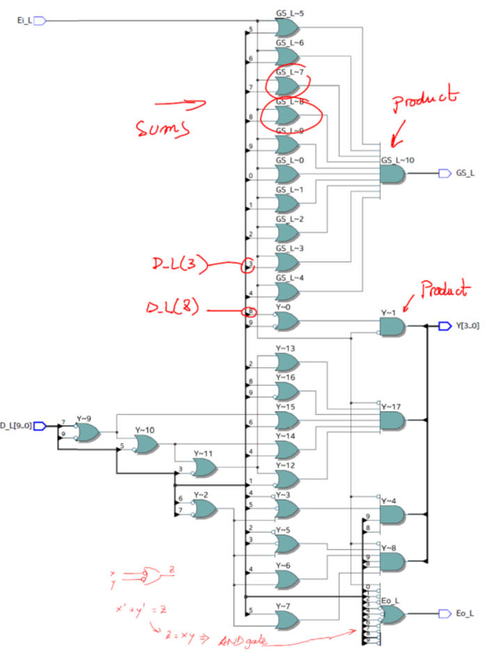
2.- Start an EDA tool project Enc_10_4_prj for a CPLD/FPGA target chip and obtain the synthesised circuit. Represent and analyse the RTL and technology views. This in Fig . 5 is an example of a RTL view of the circuit synthesised by the computer tool.
 |
|
| Fig. 7.RTL generated from the VHDL synthesis when using PoS equations. In this case, it seems quite simple to follow the circuit to check each equation. However, we'll solve the test better using a VHDL simulation. | |
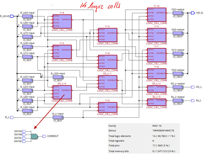
3.- Examine and print a commented copy of the technology view. Run chip planner tool to find where the used logic elements are located in the chip fabric.
 |
|
| Fig. 7.This is an example of a technology view when targeting the FPGA chip Intel MAX10 10M50DAF484C7. Study how functions are implemented for real in a programmable logic device (PLD). In this synthesis example 14 logic cells are used. | |
4. Testing
1.- Start an EDA VHDL simulator project and verify the Device-Under-Test (DUT) using a VHDL simulator test bench (Enc_4_10_tb.vhd), which may be exactly the same for all the different plans.
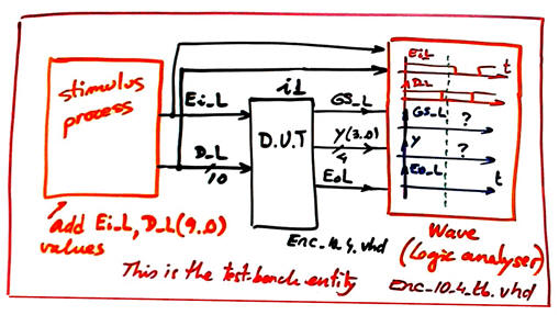 |
Fig. 8.This is the testbench schematic. The component under test is driven by input stimulus (process) and once the simulation is completed it is possible to inspect both inputs and outputs in a logic analyser (wave). |
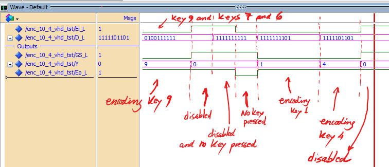
2.- Verify applying sufficient test vectors that the device works as expected (verify the truth table). Print timing diagram screen and add comments on the signals to show how the device works.
 |
|
Fig. 9. This is an example of a functional simulation of the Unit Under Test (UUT). |
5. Report
It is required a handwritten original project report containing sections 1 - 2 - 3 - 4, scanned figures with annotations, file listings, diagrams, sketches or any other resources. Theory stuff to comprehend how the circuit works may be included in section 1 on specifications.
6. Prototyping
Use training boards and perform laboratory measurements to verify how the circuit works for real. The configuration file has to be downloaded into the target board as explained in the flow chart.
| Home Term 26/27-Q1 Contact Products Electronic devices and companies Software Books Magazines Instruments DEE Library EETAC DEEL |

|
|
| Web activa des de 09/2001, @ F. J. Robert, Web editat amb Microsoft Expression Web 4. El contingut és un complement als materials d'estudi del curs Circuits i Sistemes Digitals disponibles al campus digital Atenea. Llicència:Reconeixement 4.0 Internacional de Creative Commons |