|
|
Bachelor's Degree in Telecommunications Systems and in Network Engineering |
|
|
|
||
|
|
Dec_3_8: structural single-file VHDL (flat) plan A |
|
|
|
||
Binary decoder from 3 inputs to 8 outputs (type 74LS138)
1.Specifications
Design a binary decoder 3 to 8 active-high (Dec_3_8) following the plan A based on equations. Theory on decoders is introduced in L2.3. Fig. 1 shows two symbols.
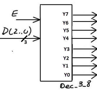
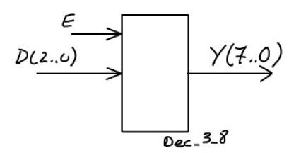 a) b) |
| Fig. 1. Dec_3_8 symbols: a) 8 independent outputs, b) vector output Y(7..0). |
As you can see, symbols may be slightly different depending on whether we decide to use vector inputs and outputs. This light difference will define the entity in VHDL and how to write equations.
In Fig. 2 there is the truth table when using vectors for both, inputs and outputs.
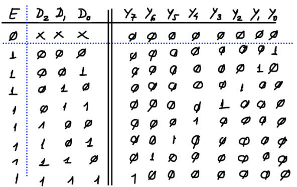 |
| Fig. 2. The Dec_3_8 truth table representing active-high inputs and outputs. |
In Fig. 3 there is an example sketch of a timing diagram. This sketch will be translated to VHDL as stimulus to drive the testbench.
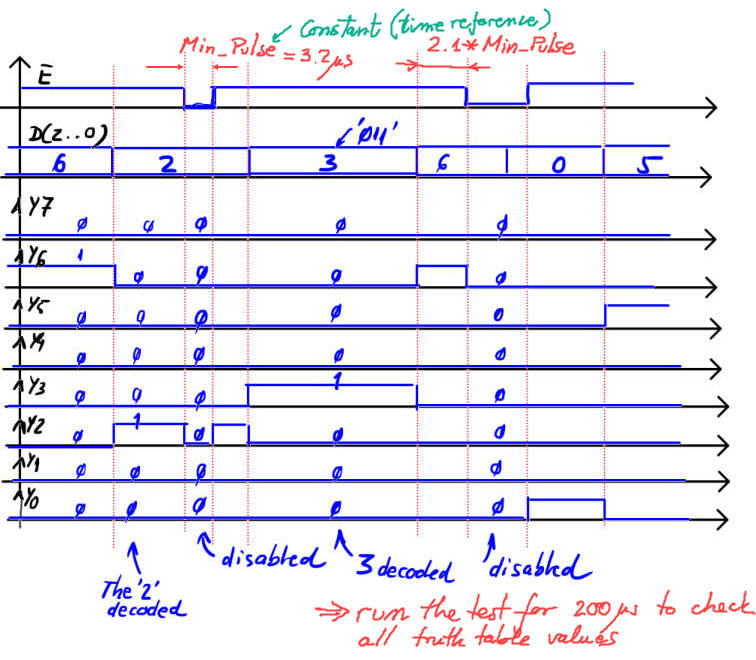 |
|
| Fig. 3. Example of a timing diagram showing some input activity and the predicted outputs for each time interval. | |
2. Planning
- Mind map representing our VHDL design flow and the main concepts involved in designing combinational circuits.
- Study the specifications in detail: symbol, truth table, special signals, commercial circuits, etc.
- For plan A, let us find a set of equations. For instance, using minilog.exe. Name the file Dec_3_8.tbl.
- Project location:
C: \CSD\P2\Dec_3_8A\(files)
- Translate SoP or PoS equations from minilog to VHDL. Name the circuit Dec_3_8.vhd.
- Start a Quartus Prime EDA project for a CPLD/FPGA target chip (Dec_3_8_prj) . Synthesise the circuit.
- Print and discuss the RTL view.
- Print and discuss the technology view. How many logic elements are used?
- Draw the VHDL testbench fixture. Generate an skeleton of testbench for the Dec_3_8. Name it Dec_3_8_tb.vhd.
- Fill in stimulus process translating input signals from the timing diagram in specifications (Fig. 3). Refer all time intervals to constant Min_Pulse.
- Test the project using a VHDL testbench and ModelSim.
- Discuss wave results. Does it work as expected?
3. Development
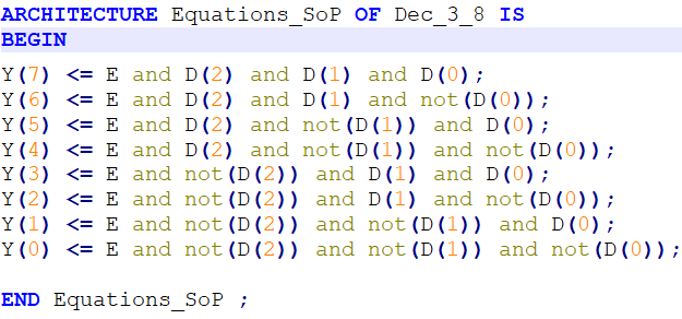
1. This is the edition of the truth table in a text file Dec_3_8.tbl. Run the minimiser and get the equation to be translated to VHDL as shown in Fig. 4.

2.- Write down the VHDL file translating the equations above. This is an example VHDL file Dec_3_8.vhd.
 |
|
| Fig. 4. Set of equations based on SoP from minilog translated to VHDL. Alternatively, this is also the set of PoS equations. | |
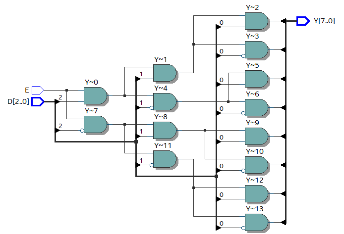
2.- Start an EDA tool project Dec_3_8_prj for a CPLD/FPGA target chip and obtain the synthesised circuit. Represent and analyse the RTL and technology views. This in Fig . 5 is an example of a RTL view of the circuit synthesised by the computer tool.
 |
|
| Fig. 5.RTL generated from the VHDL synthesis. In this case, it seems quite simple to follow the circuit to check each equation. However, we'll solve the test better using a VHDL simulation. | |
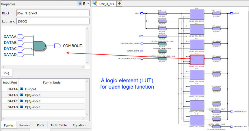
3.- Examine and print a commented copy of the technology view. Fig 6 is an example of schematic when targeting the FPGA chip Intel Cyclone IV Cyclone IV EP4CE115F29C7N. Study how functions are implemented for real in a programmable logic device (PLD).
 |
|
| Fig. 6. Technology view. | |
4. Testing
1.- Start an EDA VHDL simulator project and verify the Device-Under-Test (DUT) using a VHDL simulator test bench (Dec_3_8_tb.vhd), which may be exactly the same for all the different plans.
2.- Verify applying sufficient test vectors that the device works as expected (verify the truth table). Print timing diagram screen and add comments on the signals to show how the device works.
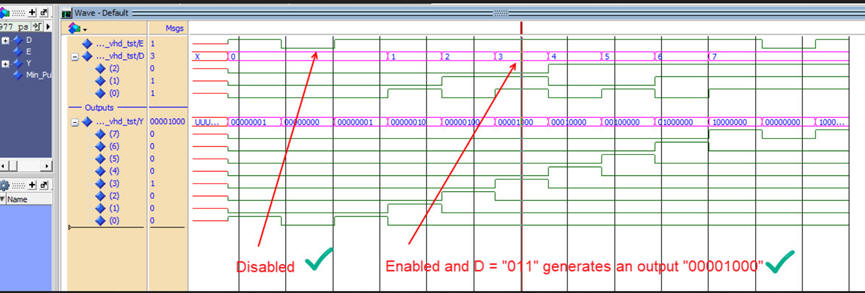 |
| Fig. 7. This is an example of a functional simulation of the Unit Under Test (UUT). |
5. Report
Project report starting with the template sheets of paper, scanned figures, file listings, docx , pptx, or any other resources
6. Prototyping
Use training boards and perform laboratory measurements to verify how the circuit works for real. The configuration file has to be downloaded into the target board.
| Home Term 26/27-Q1 Contact Products Electronic devices and companies Software Books Magazines Instruments DEE Library EETAC DEEL |

|
|
| Web activa des de 09/2001, @ F. J. Robert, Web editat amb Microsoft Expression Web 4. El contingut és un complement als materials d'estudi del curs Circuits i Sistemes Digitals disponibles al campus digital Atenea. Llicència:Reconeixement 4.0 Internacional de Creative Commons |