|
|
Bachelor's Degree in Telecommunications Systems and in Network Engineering |
|
| Analysis and design tutorials | Analysis and design assignments | Prototypes | Exam 1 | Exam 2 | Questions and assessment |
CSD EXA2: final exam examples and solution ideas |
2526Q2
Problem 1.
This is a way to start after an initial clear direct level, which have priority over CLK signals. Indicate using dots, period by period the sampled values of interest that allow to apply the flip-flop function tables. Draw this initial diagram in paper and continue for some more periods.
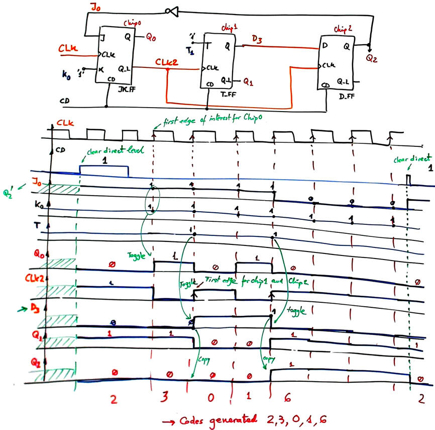
This is the experimental setup "P1_circuit.pdsprj" using analysis method II in Proteus to verify your results. Another interesting way to check the resulting waveforms is method III capturing the circuit in VHDL using plan C2.
Problem 2
1. Our dedicated processor architecture is proposed in L8.1 lecture.
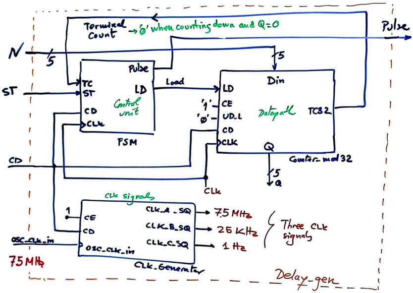
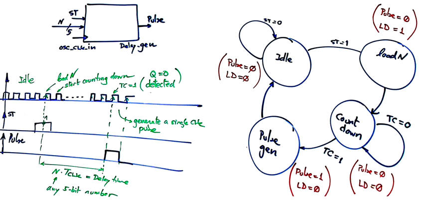
2. An example of state diagram to control the datapath and generate the Pulse output.
3. Counter expansion and and truncation. Two Counter_mod16 are chained and the count is truncated to 31. In a first design phase, this circuit is only down, which is enough for this application. It can be enhanced to make it reversible adding other components and the UD_L control signal. Expanding and truncating counters is explained in L7.3 lecture.

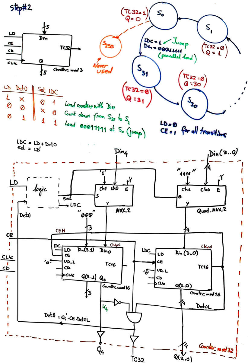
Now, before proceeding with phase #2, it is recommended to capture this circuit in VHDL and check that it works as expected using a simulation testbench.
4. The CLK_generator standard structure based on frequency dividers and T_FF is studied in L8.2 lecture. N1 = 5; N2 = 300; N3 = 25000.
5. In a synchronous system the propagation time from CLK to output is estimated considering the D_FF's CLK to output propagation time (tCO) and supposing that CC2 is a 3 level-of-gates standard combinational circuit (discussed in L6.1).
The output of interest for the user, generated by the FSM is Pulse. Its minimum duration is 9.7 ns for the maximum CLK frequency 103 MHz.
Problem 3
Basically, this application is a counter modulo 6 controlled by an start-stop push-button.
1. Init_system() will set PB0 and PB1 as inputs (TRISB = 0x03), and also another six port pins as outputs (TRISC = 0x00).
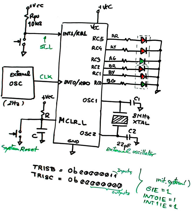
2. In this problem we can use six independent output variables, or group them by traffic lights.
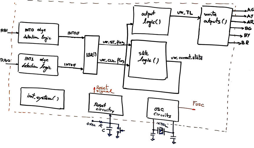
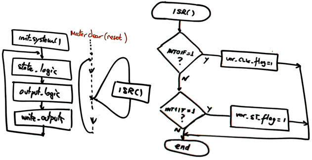
3. This traffic light application is driven by external interrupts. var_CLK_flag will allow state rotation and var_ST_flag will start and stop operations.

To validate this design phase, it is recommended to develop and test the circuit in Proteus adapting one of our tutorials, for instance, the Timer form LAB11.
4. In a second phase, var_CLK_flag will be generated by TMR0 overflows, allowing assignments of different time periods TP per colour pattern, as it has to work in street intersections.
For instance, as studied in L12.2 for the TMR0 in 8-bit mode, TP = 60 s = TB · N1 · N2 · N3
TB = 500 ns (8 MHz external quartz crystal oscillator); prescaler N1 = 256; timer N2 = 250; and the software postscaler N3 = 1875, an uint_16t RAM variable. It generates a timer hardware interrupt flag TMR0IF every 32 ms.
| Home Term 26/27-Q1 Contact Products Electronic devices and companies Software Books Magazines Instruments DEE Library EETAC DEEL |

|
|
| Web activa des de 09/2001, @ F. J. Robert, Web editat amb Microsoft Expression Web 4. El contingut és un complement als materials d'estudi del curs Circuits i Sistemes Digitals disponibles al campus digital Atenea. Llicència:Reconeixement 4.0 Internacional de Creative Commons |