| | ||
PLA3: Designing arithmetic and logic circuits using hierarchical multiple-file plan C2 |
||
| NOTE: This post-lab assignment must be solved only after having completed successfully lab session Lab3 because you will copy and adapt materials from it. |
Specifications
| Example of group assignments | ||||
| Number, entity to design | Architecture plan C2 options | Target chip options | Test vectors options | |
| Group 1 | D1.12 16-bit comparator for integer numbers | Comp_16bit:#1 Comp_4bit: #1 Comp_1bit: #1 |
#1 | #1 |
| Group 2 | D1.14 9-bit parity generator, parity checker | DeMUX_16: #1 Dec_4_16: #1 |
#2 | #1 |
| Group 3 | D1.15 3-digit code converter from BCD to binary radix-2 | DM184: #1 | #1 | #1 |
| Group 4 | D1.12 16-bit comparator for integer numbers | Comp_16bit:
#2 Comp_4bit: #2 |
#2 | #2 |
| Group 5 | D1.14 9-bit parity generator, parity checker | DeMUX_16: #2 Dec_4_16: #2 |
#1 | #2 |
| Group 6 | D1.15 3-digit code converter from BCD to binary radix-2 | DM184: #2 | #2 | #2 |
| Group 7 | D1.12 16-bit comparator for integer numbers | Comp_16bit:#1 Comp_4bit: #1 Comp_1bit: #4 |
#1 | #3 |
| Group 8 | D1.14 9-bit parity generator, parity checker | DeMUX_16: #3 Dec_4_16: #3 |
#1 | #3 |
| ··· | ··· | |||
This group submission at Atenea includes the report in a PDF file, the zipped project, a 10 min. max video presentation and also your self-assessment.
Notes on how to write and organise your report:
PLA3 written report sections:
1. Specifications and theory
Original handwritten materials on symbol, truth table, timing diagram and other explanations on data types and operations to be performed. Include example on how the circuit operate, use the corresponding radix to make for easy interpretation of the operands and results. Explain the meaning and the function of each input and output and the data range.
2. Planning
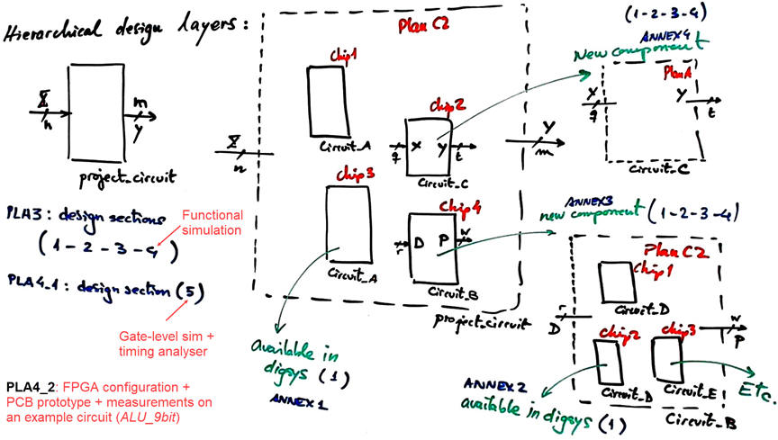
Original handwritten sketches, explanations and VHDL-ready schematics on how your plan C2 circuit is conceived, the proposed hierarchy of components, signals, number of VHDL files, project folders and names, etc. Explain what is the task assigned to each group member so that everyone is learning everything at the same time you are studying for exams. Explain how your large hierarchical project is divided in (A) top entity and (B) components (to be designed separately in annexes if they cannot be found in products). Explain which component you will solve (1-2-3-4) firstly to get some practice with the tools and the plan C2 before designing other components or assembling the top entity. This slide may give you a better idea:

3. Development
Top project development in Quartus Prime for a target FPGA chip. Printings and handwritten discussions of RTL and technology schematics. How many FPGA resources (logic cells, logic elements, etc.) are used?
4.Test and verification
Testbench fixture schematic, proposed stimulus testbench process. Printings and handwritten discussions on results. Add your conclusions on the project and on what has been learned. Remember that your self-assessment is expected to be submitted as well at the Atenea platform.
5. Annexes
If you invent a new component that is not available in products, the best way to report it is as an annex organised as a complete project. If you use the VHDL files from a component already available in digsys, you simply need to describe it in a single sheet as symbol and truth table (specifications).
Notes on video presentations: 10 min. max., 3 - 4 min. each participant.
The idea of the video presentation is different from the written report and has its own particular objective: develop your oral communications skills in our engineering context. Put in motion your communication skills that you will continue to practise and improve through PLA6_7 and PLA10_11. We will focus assessment in how you are organising the presentation, how confident you are in front of the camera, time sharing among students, support materials, time distribution and audio and video quality. This is an example of final PLA11 presentation. A good idea is to submit a meet recording or equivalent.
| ===> Do not browse your report pages when presenting, prepare some slides instead. |


