|
|
Bachelor's Degree in Telecommunications Systems and in Network Engineering |
|
|
|
|||||
Chapter 2 problems |
- A2.4 - |
Analysis of an asynchronous circuit |
|||
|
|
|||||
1. Specifications
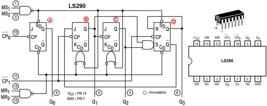
Fig. 1 represents the datasheet schematic of the chip 74LS290 containing several chained flip-flops and logic gates. Let us adapt it as usual to our naming style and conventions.
 |
|
Fig. 1. 74LS290 chip and its internal circuit. |
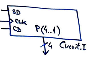
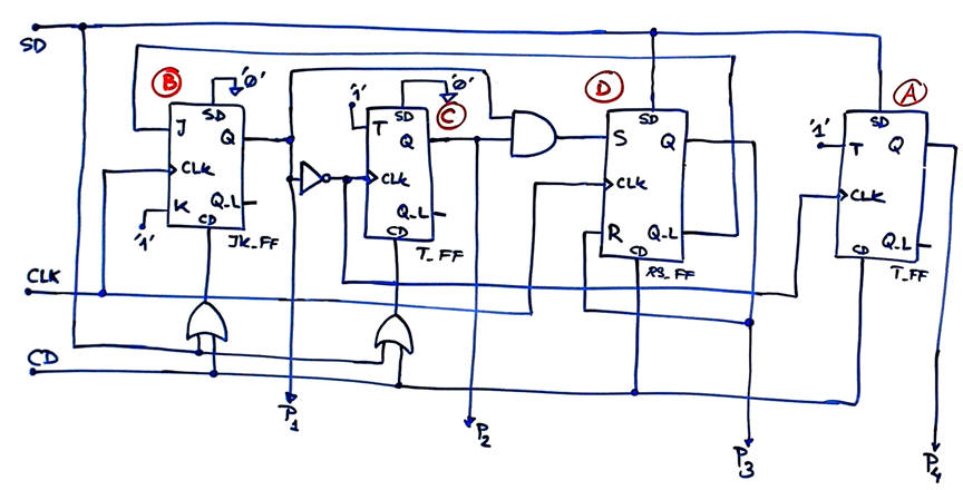
We can use our set of tools to analyse Circuit_I represented in Fig. 2 built using this chip and connecting its pins. We have used our drawing style and naming conventions identifying the different flip--flops included in the chip.
  |
|
Fig. 2. Circuit_I symbol and schematic built using the 74LS290 chip. |
Determine how does the Circuit_I work, finding the output vector P(4..1) using our three analysis methods.
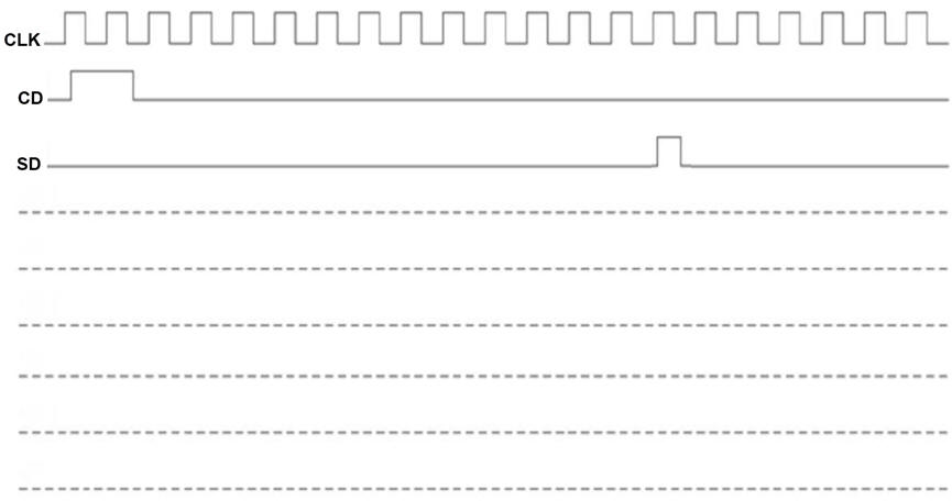
A convenient waveform template is shown in Fig 3.
 |
|
Fig 3. Waveforms template. |
Discuss how many states the system is capable of memorising.
Discuss what may be the function or application of the circuit, if any.
Measure propagation delay CLK to output (tCO) and deduce the maximum CLK frequency fMAX that can be applyed to the circuit.
As we proposed in P1 analysing combinational circuits, self-assess the validity of your solution comparing results obtained from different methods.
2. Planning
Method I. Handwritten analysis to draw the circuit's timing diagram and determining the outputs. In LAB5 session we fixed a procedure consisting of several steps.
Use this project location to save your paper solution, class notes, pictures, theory, etc.:
C:\CSD\P5\Circuit_I\paper\(files)
Method II. Proteus capture and electrical simulation. Apply the planned stepped procedure in LAB5 capturing and analysing your circuits to get experience using Proteus and its new components and instruments. Find circuits to copy and adapt using the corresponding library of components.
Proteus components library options:
option #1: LS-TTL
option #2: CMOS
Project location:
C:\CSD\P5\Circuit_I\proteus\(files)
Method III. VHDL synthesis and simulation. Apply the planned stepped procedure in LAB5 to use correctly our VHDL EDA tools and find the flip-flop components in our tutorials (D_FF, JK_FF, T_FF).
CPLD or FPGA target chip options:
option #1: MAX II
option #2: Cyclone IV
Synthesise the project and print the RTL view. Be aware that the "number of registers" in the project's summary spreadsheet must be correct.
Use a VHDL test bench to demonstrate that the timing diagram looks like that obtained in the previous analysis methods.
How can you observe and measure glitches, false states and complications around CLK transitions?
Project location:
C:\CSD\P5\Circuit_I\VHDL\(files)
Optional. Exercise related to the next P6 content: How to implement the same application using a standard synchronous circuit? Design an FSM to generate synchronously the same output P(4..1).
| Home Term 24/25-Q1 Contact Products Electronic devices and companies Software Books Magazines Instruments DEE Library EETAC DEEL |

|
|
| Web activa des de 09/2001, @ F. J. Robert, J. Jordana. Web editat amb Microsoft Expression Web 4. El contingut és un complement als materials d'estudi del curs Circuits i Sistemes Digitals disponibles al campus digital Atenea. Llicència:Reconeixement 4.0 Internacional de Creative Commons |