|
|
Bachelor's Degree in Telecommunications Systems and in Network Engineering |
|
|
|
|||||
Chapter 2 problems |
- A2.2 - |
Analysis of an asynchronous circuit (Circuit_A) |
|||
|
|
|||||
1. Specifications
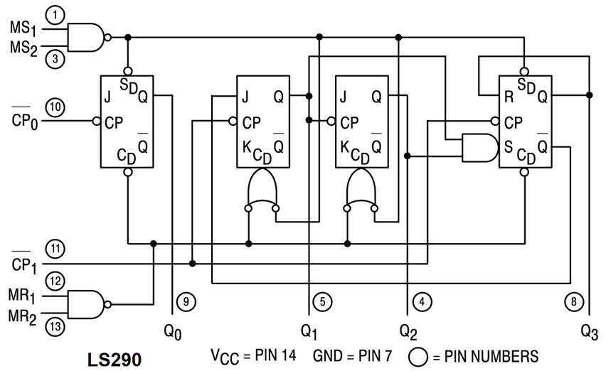
Fig. 1 represents the internal circuit of chip 74LS290 containing several chained flp-flops and logic gates from its datasheet. Let us adapt it as usual to our naming style and conventions.
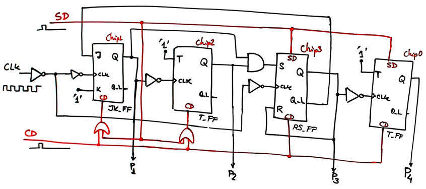
We can use our set of tools to analyse Circuit_A represented in Fig. 2 built using this chip resources and external logic gates.
 |
|
Fig. 1. 74LS290 chip equivalent internal circuit. |
Read its datasheet to determine how does it work (what is the funcion of each pin). Some J and K inputs are not driven, we will assume that they are connected to '1'.
Analyse Circuit_A in Fig. 2 using method II: Proteus capture and simulation, or method III: VHDL synthesis and test. Determine how does the circuit work, meaning finding the vector output P(4..1) in a clocked (CLK) timing diagram.
What is the maximum CLK frequency when picking the PLD target chip indicated below?
- Cyclone IV
- MAXII
Test your solutions using method I: handwritten analysis.
 |
|
Fig. 2. Circuit_A to be analysed using our three methods. |
Hint: Suggested step-by-step plan to solve this kind of analysis projects A2.1, ..., A2.7:
Like in P1 analisys, each method has its own organisation 1-2-3-4. Section 1 is the same for all methods, and section 4 is a paragraph says something like "The circuit solved using method 1 generates the same result that method 2" and conclusions.
A. Solve a circuit with only one FF. Use a section of the circuit in Fig. 2 or any tutorial D_FF, JK_FF (and also RS_FF), T_FF.
This is determining the outputs using two (or even the three) methods and compare solutions. Your aim is to learn new concepts and ideas such:
- What values are sampled?
- When the circuit sample? When the circuit is doing nothing?
- When the outputs are going to switch? Why?
- What is the output pattern? Is it a single event or a periodic signal?
Using method 2, you have to find components in CMOS or TTL-LS technologies to capture your circuit. It is recommended to use this Proteus circuit to copy and adapt. Use the logic analyser instrument and learn about triggering (arming) waveform captures. Change colour for better printing results. Comment the waveforms.
Using method 3, you have to find VHDL components in tutorials D_FF, JK_FF, T_FF. And build using plan C2 the top circuit including logic gates if necessary. Draw a new schematic annotating every signal and chip to be able to translate it to VHDL and develop the project.
Using method 1, basically you try to learn how to generate timing diagrams like the ones shown in specifications in tutorials D_FF, JK_FF, T_FF..
B. Solve a circuit with rong>two CLK. Use a section of the circuit in Fig. 2 or invent or find any other circuit.
ThiThis step is fundamental because you will learn what to do when outputs are switching at different times. What values are sampled? When? What is the output pattern? How many states (output combinations) the circuit will have? Does it generate a periodic signal or a single not repetitive event?
C. Now you are ready for solving the circuit proposed in Lab5 reproducing a timing diagram as in Fig. 3 from the three methods.
D. Solve the circuit in Fig. 2 using all the resources learned in previous steps answering similar questions.
| Home Term 24/25-Q1 Contact Products Electronic devices and companies Software Books Magazines Instruments DEE Library EETAC DEEL |

|
|
| Web activa des de 09/2001, @ F. J. Robert, J. Jordana. Web editat amb Microsoft Expression Web 4. El contingut és un complement als materials d'estudi del curs Circuits i Sistemes Digitals disponibles al campus digital Atenea. Llicència:Reconeixement 4.0 Internacional de Creative Commons |