|
|
Bachelor's Degree in Telecommunications Systems and in Network Engineering |
|
|
|
Radix-2 synchronous counter modulo 12 using plan X |
FSM application enumerating states
| 1. Specifications | Planning | Developing | Test functional | Test gate-level | Prototype | Report |
Design the synchronous Counter_mod12 represented in Fig. 1 using plan X.
 |
 |
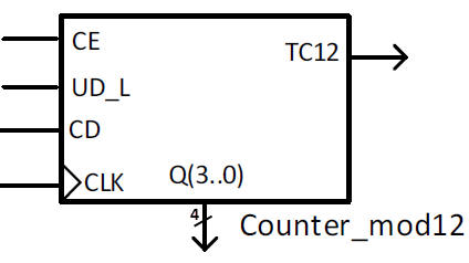
| Fig 1. Symbol and function table. |
|
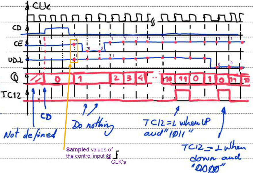 |
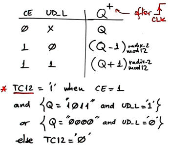
Fig 2. Example of timing diagram. |
The aim is to compare its design and architecture with alternative designs when implementing the same circuit using plan Y and plan C2 proposed at Lab7.
 |
Fig. 3. State diagram representing the 36 state transitions and outputs. |
| Specifications | 2. Planning | Developing | Test functional | Test gate-level | Prototype | Report |
Plan X: FSM strategy as in P6 (naming all the states and State_type signals). This approach is possible because it is a sequential circuit with only a few states and a few state transitions that can be enumerated easily as with other FSM.
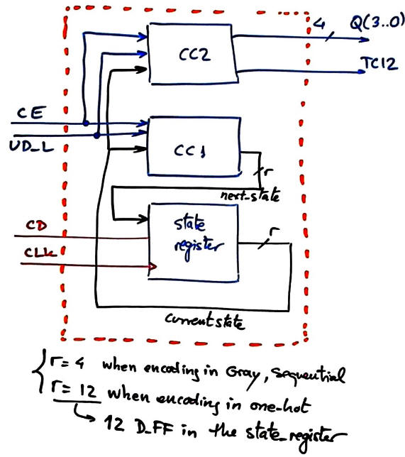 |
Fig. 4. FSM to implement the Counter_mod12 using plan X. |
We will follow the procedure for designing FSM.
Project location:
C:\CSD\P7\Counter_mod12X\Counter_mod12.vhd, etc.
| Specifications | Planning | 3. Developing | Test functional | Test gate-level | Prototype | Report |
Some example of files for developing the circuits:
To obtain the Counter_mod12.vhd file copy and adapt for example the Counter_BCD_1digit.vhd.
 |
Fig. 5. RTL view |
|
|
Fig. 6. State diagram interpreted by Quartus Prime, encoded in one-hot (12 D_FF are required). |
|
|
Fig. 7. Technology view schematic for a MAX II Intel CPLD. |
| Specifications | Planning | Developing | 4. Test functional | Test gate-level | Prototype | Report |
Start the test bench template and add the CLK and inputs activity translating the timing diagram. Make all the timing relative to the CLK_Period constant.
|
|
Fig. 8. Testbench schematic fixture. |
This is an example VHDL file translation from which you can copy the CLK_Period constant, and also the stimulus and CLK processes Counter_mod12_tb.vhd. You can use the same testbench that was written for the other plan Y and plan C2.
Functional simulation. Run the EDA VHDL tool and demonstrate how the circuit works adding comments to the printed sheet of paper containing the waveforms. Your system may works like the timing diagram discussed in class.
 |
Fig 9. Example of a functional simulation of the counter module 12. |
| Specifications | Planning | Developing | Test functional | 5. Test gate-level | Prototype | Report |
Gate-level simulations in ModelSim
Run the gate-level simulation of the project and measure the maximum frequency of operation. It is worth to know exactly which is the maxim CLK frequency for a given target CPLD or FPGA chip.
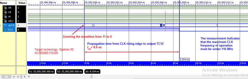 |
| Fig 10. Example of a gate-level simulation of the counter modulo 12 used to measure the parameter tCO in a given CLK transition. |
Quartus Prime timing analyser
Timing analyser spreadsheet to measure tCO.
| Specifications | Planning | Developing | Test functional | Test gate-level | 6. Prototype | Report |
Practice with the example proposed in this version of the counter.
| Specifications | Planning | Developing | Test functional | Test gate-level | Prototype | 7. Report |
Follow this rubric for writing reports.
| Home Term 26/27-Q1 Contact Products Electronic devices and companies Software Books Magazines Instruments DEE Library EETAC DEEL |

|
|
| Web activa des de 09/2001, @ F. J. Robert, Web editat amb Microsoft Expression Web 4. El contingut és un complement als materials d'estudi del curs Circuits i Sistemes Digitals disponibles al campus digital Atenea. Llicència:Reconeixement 4.0 Internacional de Creative Commons |