|
|
Bachelor's Degree in Telecommunications Systems and in Network Engineering |
|
| Analysis and design tutorials | Analysis and design assignments | Prototypes | Exam 1 | Exam 2 | Questions and assessment |
CSD EXA2: final exam examples and solution ideas |
2526Q1
Problem 1.
This is a way to start, period by period, noticing the sampled values of interest that allow to apply flip-flop function tables. Draw this initial diagram in paper and continue for some more periods.
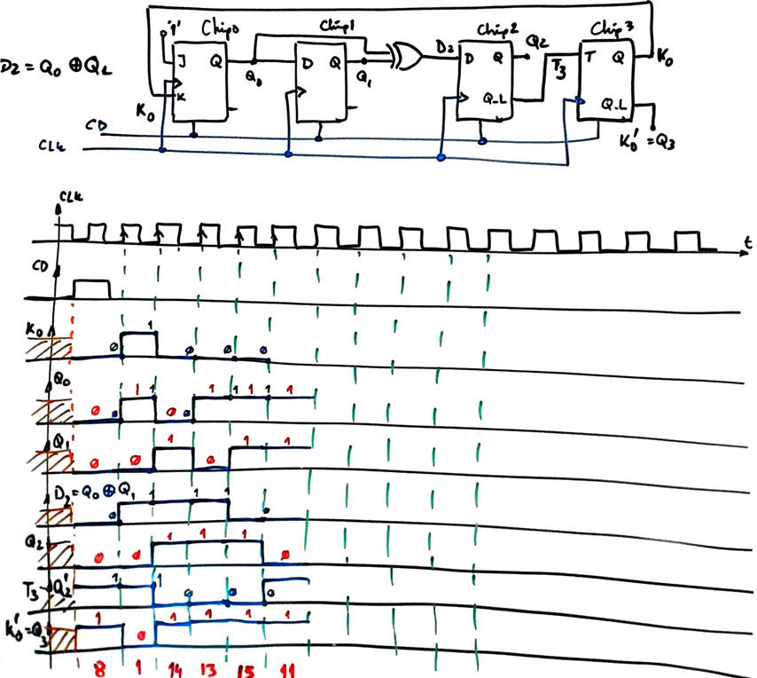
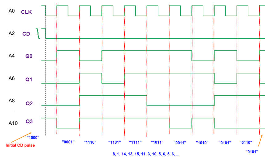
Example solution using method 2 in Proteus displaying only the outputs to check the codes generated by the circuit. The logic analyser is triggered on the falling edge of the CD signal. You can practise with it, for instance, add other channels to visualise the complete set of nine signals of interest, pay attention to flip-flop inputs sampled values.
b) You need to name all signals and chip references (Chip0, Chip1, etc.), and also add a buffer for each output that is used for internal logic. Try this method 3 and compare with method 1 and method 2.
Problem 2
This is an starting point. Complete the diagrams in your paper.
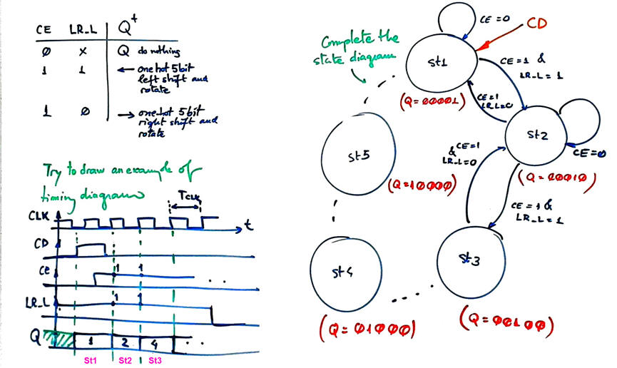
Now you can continue this problem:
A) Apply the plan C1 FSM recipe described in the lecture L6.1 or P6 or LAB6.
B) Apply plan C2 and counter truncation as described in L7.3 or P7 or LAB7.
NOTE: You can even imagine a third strategy on plan C2 using standard shift registers as described in L7.3. How to connect and control them in order to generate the sequence of five states required in this application?
Develop your plan for the circuit in VHDL targeting a MAX10 FPGA, prototype it and measure the waveforms using our VB8012 instrument.
Problem 3
This is a way to start. The key idea here is to detect the PB rising edge by means of an external interrupt. The ISR() will set the convenient variable var_PB_flag to control state transitions. The interrupt mechanism allows to solve the problem only in three states. Discuss the comparison with the hardware version in VHDL at LAB6.
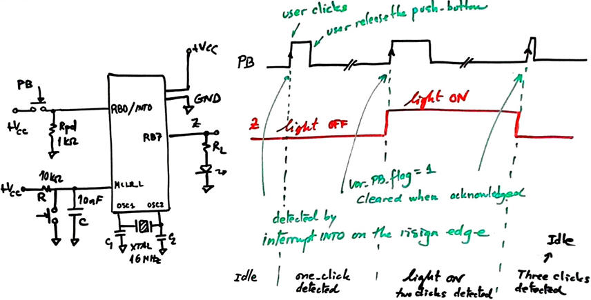
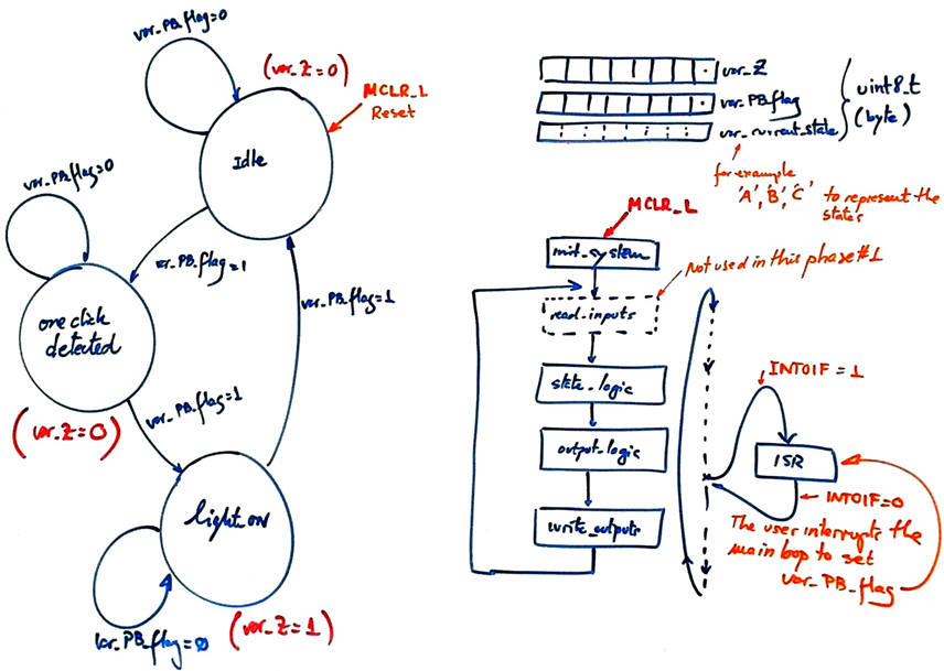
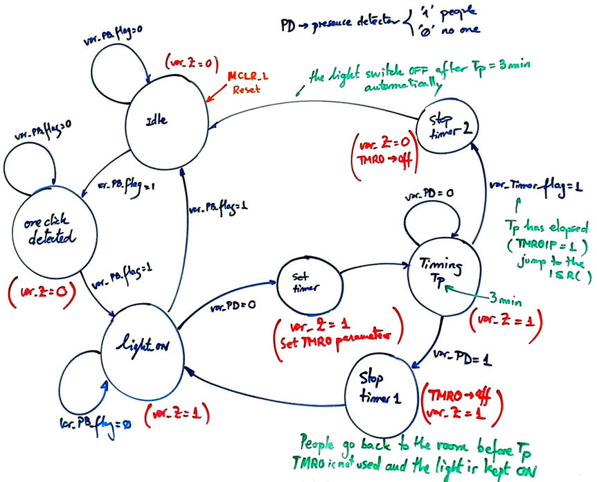
You can always enhance your product adding new states to control the timer device that will switch off the light in people are not detected in the room for 3 min. The presence detector can be read while on light_ON. However, to develop and test this new design phase, remember that the design phase #1 has to be fully operational.
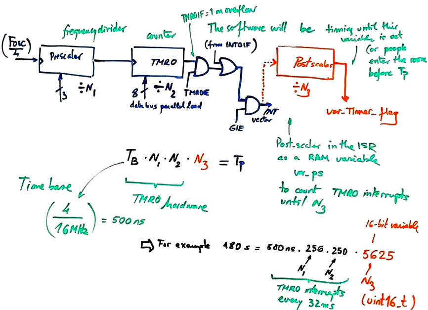
The main ideas on configuring the TMR0 peripheral to generate the new required interrupt var_Timer_flag are shown in the diagram below. To time 180 s requires the use of a software RAM variable postscaler type uint16_t. In LAB11 you can find examples of diagrams and C code.
| Home Term 26/27-Q1 Contact Products Electronic devices and companies Software Books Magazines Instruments DEE Library EETAC DEEL |

|
|
| Web activa des de 09/2001, @ F. J. Robert, Web editat amb Microsoft Expression Web 4. El contingut és un complement als materials d'estudi del curs Circuits i Sistemes Digitals disponibles al campus digital Atenea. Llicència:Reconeixement 4.0 Internacional de Creative Commons |