|
|
Bachelor's Degree in Telecommunications Systems and in Network Engineering |
|
|
|
|||||
Chapter 2 problems |
- D2.8 - |
Electronic keypad lock (FPGA-VHDL) |
|||
|
|
|||||
1. Specifications
Let us design an electronic keypad lock that requires a numerical code or password in order to unlock the door, thus no need of physical keys. Although they are more expensive than most kind of locks, your security is well-ensured. It is important that you keep your numerical code or password safe and difficult for outsiders to guess.
The same project designed programming a μC is in D3.8.
 |
|
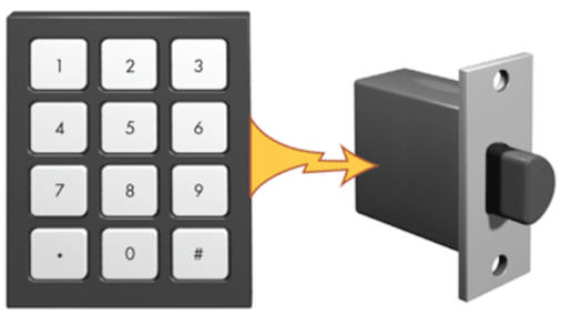
Fig. 1. The idea of an electronic keypad lock. References about these concepts and commercial products are everywhere, for instance: https://www.nokey.com or https://www.embedded.com/using-finite-state-machines-to-design-software. |
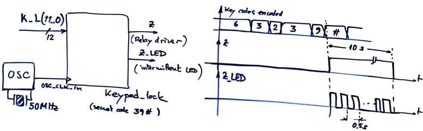
The symbol of such circuit will consider an output Z for driving an electromechanical relay during a 10 s period, and also another intermittent Z_LED (2 Hz) that is during the open door period. Keypads can be connected using a combinational circuit or a sequential matrix. Showing in 7-segment displays the digits currently being clicked may be an option.
 |
|
Fig. 2. Example of symbol and idea of waveforms when the secret code is detected. In this picture, as an example, the secret code is three digit "39#", but it can be of any number of symbols. |
2. Planning
We can propose two alternative options to design the circuit.
Option #A: A FSM with some additional circuits. The idea is to examine only one digit at a time and be able to advance when the current digit is correct, similarly as we did in the pattern detector circuit D2.4.
In this design we will embed the password "39#" to open the door in hardware. Invent the electronic circuit for conditioning the keypad and driving the door motor. See Fig. 3. The encoder may be a combinational from Chapter I (DT2.5, L2.3), or a matricial FSM as proposed in the highlighted project P6.
 |
|
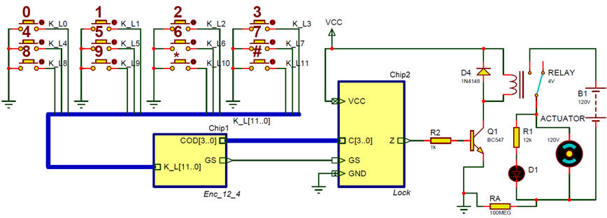
Fig. 3. Schematic in Proteus to get ideas on the control system Keypad_lock. The relay is switched ON when Z = '1'. |
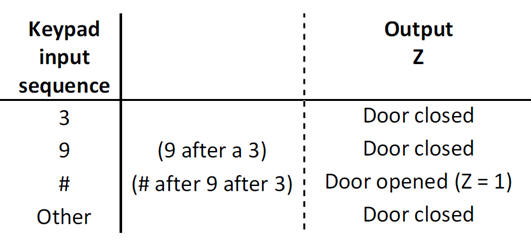
As represented in Fig. 4, the latch will open only after having sampled the correct sequence of three numbers.
 |
|
Fig. 4. Sequence for unlocking the latch. |
Sketch a timing diagram showing the main operations.
Adapt the FSM architecture to this problem, naming and connecting all signals and inputs and outputs.
Infer and draw the circuit's state diagram. Annotate all the state transitions and outputs.
 |
|
Fig. 5. State diagram. |
Deduce how many D_FF are required when encoding FSM states using the following options and draw the state register memory:
Option #1: radix-2 (sequential)
Option #2: Gray
Option #3: Johnson
Option #4: one-hot
How many D_FF will include the complete application?
Draw the FSM state register memory block.
Draw the CC2 truth table to obtain the outputs of the circuit and its flowchart.
Draw the CC1 truth table to handle state transitions (arrows) and its equivalent flowchart.
Project location:
C:\CSD\P7\lock_A\(files)
Write the FSM VHDL file. Start a Quartus Prime synthesis project for one of the following programmable target chips:
Option #1: Cyclone IV EP4CE115F29C7
Option #2: MAX II EPM2210F324C3
Option #3: MAX 10 10M50DAF484C7
Write a VHDL test bench and run the EDA simulation tool to verify your design.
The system works with a 200 Hz CLK frequency derived from a crystal quartz oscillator of 50 MHz. Add a CLK_generator circuit.
Optional design phase #2: Add another timer to the keypad lock (or make the one used for timing 10 s programmable) so that if the right sequence is not entered in 30 s, the system reset automatically.
Option #B: A dedicated processor architecture: the datapath capture the last four digits clicked and compare with the internal secret code. Indeed, it can be designed using any secret code lenght.
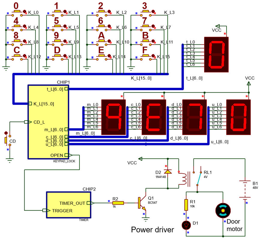
The Fig. 6 below shows an example of this version of electronic keypad lock that requires a 4-digit secret password in order to unlock the door. In this case the secret code is set using 16 switches to form 4 hexadecimal symbols (for instance "13B7"). This design Keypad_lock.pdsprj solved in Proteus allows playing with the application and studying its internal architecture. The lock mechanism is connected to an electromechanical relay, a power transistor and a 10 s timer. Several 7-segment digits show the digit currently being pressed and the saved symbols while typing the secret key.
 |
|
Fig. 6. Electronic lock circuit example in Proteus to get ideas. |
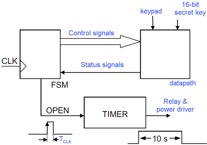
Design this application as a dedicated processor with control unit (FSM), datapath and CLK_Generator (Fig. 7).
 |
|
Fig. 7. Block diagram of a dedicated processor. The timer can be included as another component of the datapath. The CLK_generator is not shown. |
Datapath: Find ideas and tutorial examples on how to design the datapath for this application. What components will be required?
CLK_Generator. The system works with a 200 Hz CLK frequency derived from a crystal quartz oscillator of 50 MHz. Design the CLK_generator circuit.
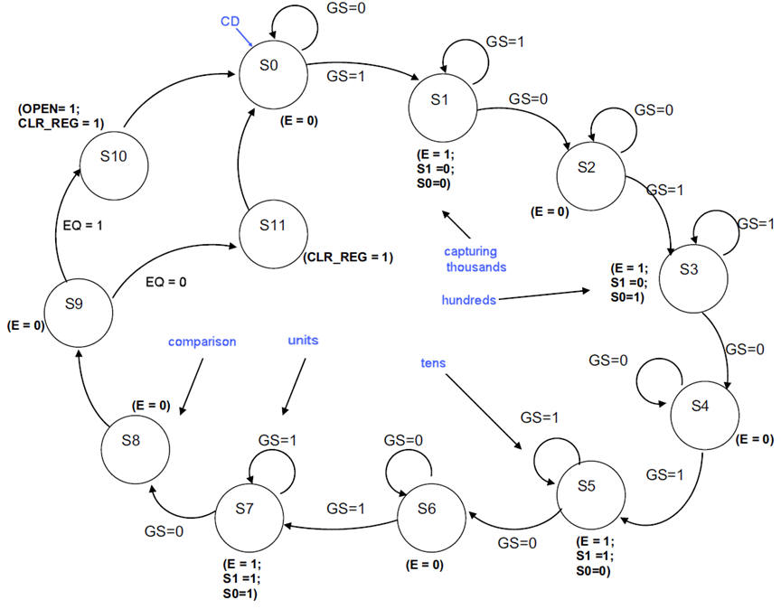
Control unit: Design the FSM . If you adapt the Proteus example, the state diagram represented in Fig. 8 may be used to drive control signals deduced from the Proteus circuit. OPEN = '1' only at state S10; other states OPEN = '0'; CLR_REG = '1' only at S10 and S11; other states '0'. Other signals not indicated are 'x'.
 |
|
Fig. 8. Example of state diagram associated to the Proteus circuit. |
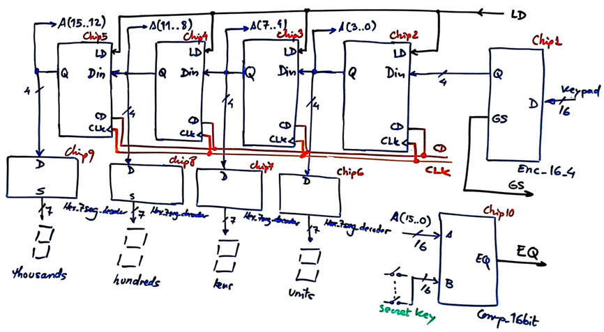
An alternative convenient design option to simplify the datapath (and also the FSM's state diagram) from the one studied in the Proteus example above, is to input keys as in a calculator, shifting digits from right to left. A single control signal LD from the FSM will load and shift left input data. After having captured 4 digits the number can be compared to the secret key. This idea is also introduced in the timer downcounter in D2.13.
 |
|
Fig. 9. An alternative datapath for capturing and left shifting. |
Project location:
C:\CSD\P7\lock_B\(files)
Deduce how many D_FF are required when encoding the control unit FSM states using the following options and draw the state register memory:
Option #1: radix-2 (sequential)
Option #2: Gray
Option #3: Johnson
Option #4: one-hot
How many D_FF will include the application dedicated processor?
Write the FSM VHDL file. Start a Quartus Prime synthesis project for one of the following programmable target chips:
Option #1: Cyclone IV EP4CE115F29C7
Option #2: MAX II EPM2210F324C3
Option #3: MAX 10 10M50DAF484C7
Write a VHDL test bench and run the EDA simulation tool to verify your design.
Optional design phase #2: Add a timer to the keypad lock so that if the right sequence is not entered in 30 s, the system reset automatically.
Optional design phase #3: If the wrong sequence is inputted after three consecutive trials, the system goes blocked. Security staff will unblock the system clicking a second secret key of two digits.
| Home Term 24/25-Q1 Contact Products Electronic devices and companies Software Books Magazines Instruments DEE Library EETAC DEEL |

|
|
| Web activa des de 09/2001, @ F. J. Robert, J. Jordana. Web editat amb Microsoft Expression Web 4. El contingut és un complement als materials d'estudi del curs Circuits i Sistemes Digitals disponibles al campus digital Atenea. Llicència:Reconeixement 4.0 Internacional de Creative Commons |