|
|
Bachelor's Degree in Telecommunications Systems and in Network Engineering |
|
|
|
|||||
Chapter 3 problems |
- D3.4 - |
Designing a pattern detector (μC - C) |
|||
|
|
|||||
1. Specifications
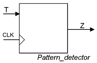
Our aim is to implement a circuit to detect the binary pattern "0110" received from a radio transmitter bit stream at input T using a microcontroller PIC18F4520, C language and our programming style. Fig. 1 shows the symbol of this pattern_detector circuit.
The same project designed using hardware is stated in D2.4.
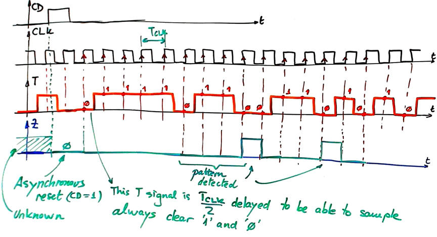
When the sequence "0110" is detected output Z goes high for one CLK period. Two or more adjacent patterns can also be detected as in this bit stream sequence: "01101101101..."
To make it a simple FSM design, we will assume:
- The bitstream incoming frequency is the same of the pattern_detector CLK.
- The bit stream signal is delayed half period with respect the CLK, to be able to sample stable data every CLK rising edge.
-- Transmission is continuous.
Design phase #1 Basic pattern detector circuit.
 |
|
Fig. 1. Symbol. |
The best way to start, is to try imagining how the output will be for a given bitstream, as represented in Fig. 2.
 |
|
Fig. 2. Example of timing diagram. fCLK = 75 Hz. |
Some questions to kick off the project and organise it as a FSM in four sections:
Project location:
C:
A) Planning hardware
Copy and adapt a circuit from a convenient tutorial project and name it Pattern_detector.pdsprj. Assign pins to inputs and outputs accordingly to one of the following options (your instructor will tell you which):
Pin assignment option #1:
CLK --> RB1
T --> RB6
Z --> RC7
Pin assignment option #2:
CLK --> RB2
T --> RA2
Z --> RD7
Pin assignment option #3:
CLK --> RB0
T --> RB7
Z --> RC4
Draw the hardware schematic. Buttons and switches, resistors, inputs, outputs, reset circuit MCLR_L and quartz crystal oscillator of 8 MHz. Explain how to configure inputs and outputs in init_system().
How to generate example bit streams in Proteus?
B) Planning software
Draw the flowchart of the general program organisation.
Draw the hardware/software diagram indicating the required RAM variables and how the FSM is solved in software.
Infer the state diagram governing the machine.
Explain how to poll (read) input T in read_inputs() using bitwise operations. Explain how to measure how many times per second this input is read.
Explain how to drive output pins in write_outputs().
Draw the truth tables and their equivalent flowcharts for state_logic() and output_logic() functions.
How the interrupt service routine ISR() is used in this application? Draw its flowchart.
Developing & testing (debugging)
Develop and test (debugging) the project capturing the hardware circuit in Proteus and writting the C source code.
| Note: Step-by-step tactical approach for developing and testing the project: Read one input at a time and run to check that the voltage value is correctly captured as a valid digital value in RAM memory. Write one output at a time and run to check that your code is correct to light the LED connected at the output pin. |
Design phase #2: Add an LCD to show messages, such text, for example: "no input data", "pattern detected", etc. A number will indicate the number of times the pattern is detected in the incoming bit stream.
Design phase #3: Use the TMR2 to replace external CLK interrupts.
| Home Term 24/25-Q1 Contact Products Electronic devices and companies Software Books Magazines Instruments DEE Library EETAC DEEL |

|
|
| Web activa des de 09/2001, @ F. J. Robert, J. Jordana. Web editat amb Microsoft Expression Web 4. El contingut és un complement als materials d'estudi del curs Circuits i Sistemes Digitals disponibles al campus digital Atenea. Llicència:Reconeixement 4.0 Internacional de Creative Commons |