|
|
Bachelor's Degree in Telecommunications Systems and in Network Engineering |
|
|
|
|||||
Chapter 2 problems |
- A2.8 - |
Analysis of an asynchronous circuit (Circuit_G) |
|||
|
|
|||||
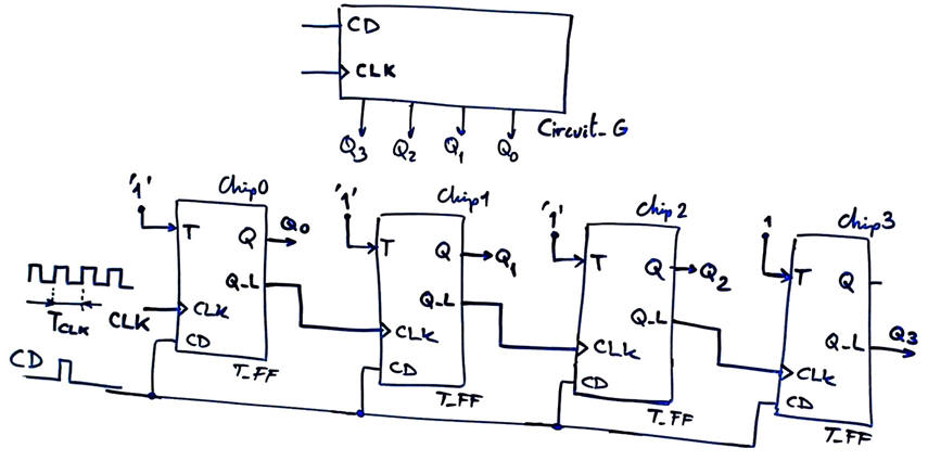
1. Specifications
The circuit represented in Fig. 1 is composed of T_FF. Let us deduce how it works by means of a timing diagram and what may be its application obtaining the output codes Q(3..0). Measure propagation delays CLK to output (tCO) and deduce the maximum CLK frequency fMAX that can be applyed to the circuit.
This is an example of an asynchronous circuit that can serve to demonstrate how complicated and unreliable is asynchronous design compared to synchronous canonical design based on FSM that is presented in the next P6.
 |
|
Fig 1. Circuit_G to be analysed using up to three methods. |
2. Planning
Method I. Handwritten analysis to draw the circuit's timing diagram.
Let us do it in two steps:
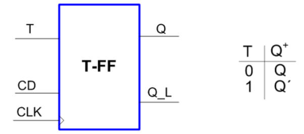
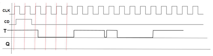
Step #1: analyse the behaviour of a single T_FF in Fig. 2 and represent the output Q in a timing diagram like the one represented in Fig.3
 |
|
Fig 2. T_FF symbol, function table and state diagram. |
NOTE: You must indicate always the T sampled values on the CLK rising edges using dots.
 |
|
Fig 3. Example input waveforms to be used as stimulus for calculating the output Q. |
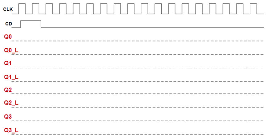
Step #2: the full circuit. Deduce the output Q(3..0) of the circuit represented in Fig. 1. The procedure to follow is presented in P5 highlighted project.
 |
|
Fig 4. Waveforms. Indicate the important CLK1, CLK2 and CLK3 signals that drive the T_FF. |
Discuss how many states the system is capable of memorising.
Discuss what may be the function or application of the circuit. What is the circuit's main problem, so that it must be rejected for precision applications?
Use this project location to save your paper work, class notes, pictures, theory, etc.:
C:\CSD\P5\Circuit_G\paper\(files)
Method II. Proteus capture and electrical simulation. In our LAB5 session you can learn some experience using Proteus and find circuits to copy and adapt using the corresponding library of components. Apply the planned stepped procedure for capturing and analysing your circuits.
Proteus components library options:
option #1: LS-TTL
option #2: CMOS
Project location:
C:\CSD\P5\Circuit_G\proteus\(files)
Method III: using VHDL synthesis and simulation tools (plan C2 circuit).
Get the component T_FF model and translate to VHDL the top circuit (Circuit_G.vhd) to be able to start a new multiple-file plan C2 project.
CPLD or FPGA target chip options:
option #1.: MAX II
option #3.: Cyclone IV
Synthesise the project and print the RTL view. Be aware that the "number of registers" in the project's summary spreadsheet must be correct.
Use a VHDL test bench to demonstrate that the timing diagram looks like that obtained in the previous analysis methods.
How can you observe and measure glitches, false states and complications around CLK transitions?
Project location:
C:\CSD\P5\Circuit_G\VHDL\(files)
Optional: Alternative canonical circuit based on FSM.
e) Design an FSM that generates the same output Q(3..0). Will it be a better replacement of the asynchronous circuit in Fig. 1?. Why?
| Home Term 23/24-Q2 Contact Products Electronic devices and companies Software Books Magazines Instruments DEE Library EETAC DEEL |

|
|
| Web activa des de 09/2001, @ F. J. Robert, J. Jordana. Web editat amb Microsoft Expression Web 4. El contingut és un complement als materials d'estudi del curs Circuits i Sistemes Digitals disponibles al campus digital Atenea. Llicència:Reconeixement 4.0 Internacional de Creative Commons |