|
|
Bachelor's Degree in Telecommunications Systems and in Network Engineering |
|
|
|
|||||
Chapter 2 problems |
- A2.7 - |
Analysis of an asynchronous circuit (Circuit_C) |
|||
|
|
|||||
1. Specifications
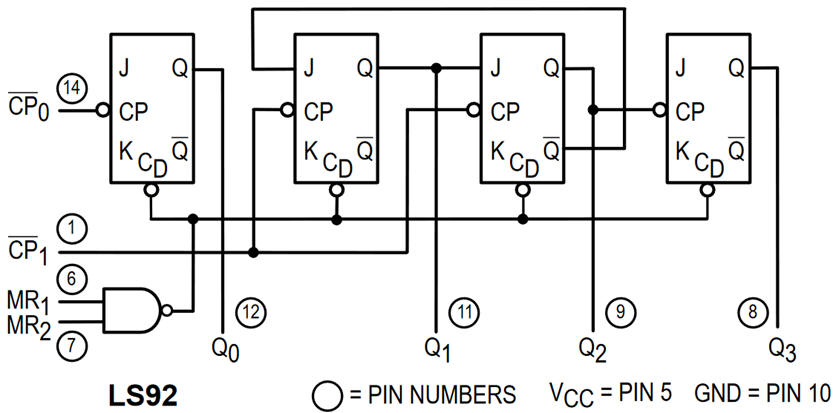
Fig. 1 represents the internal circuit of chip 74LS92 containing several chained flip-flops from its datasheet. Let us adapt it as usual as shown in Fig. 2 to our naming conventions and styles.
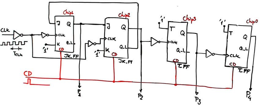
We can use our set of tools to analyse Circuit_C represented in Fig. 2 built using this chip resources and external logic gates.
 |
|
Fig. 1. 74LS92 chip equivalent internal circuit. |
Read its datasheet to determine how does it work (what is the funcion of each pin). Some J and K inputs are not driven, let us assume that they are connected to '1'.
 |
|
Fig. 2. Circuit_C to be analysed using our three methods. |
Determine how does the circuit work, meaning finding the vector output P(4..1) in a clocked (CLK) timing diagram using our three analysis methods. Measure propagation delays CLK to output (tCO) and deduce the maximum CLK frequency fMAX that can be applyed to the circuit.
Method I. Handwritten analysis.
In two analysis steps: firstly analyse only one JK_FF, secondly, the complete circuit.
Discuss how many states the system is capable of memorising.
Discuss what may be the function or application of the circuit. What is the circuit's main problem, so that it must be rejected for precision applications?
Use this project location to save your paper work, class notes, pictures, theory, etc.:
C:\CSD\P5\Circuit_C\paper\(files)
Method II. Proteus capture and simulation using CMOS or LS-TTL technology components. In our LAB5 session you can learn some experience using Proteus and find circuits to copy and adapt using the corresponding library of components. Apply the planned stepped procedure for capturing and analysing your circuits.
Proteus components library options:
option #1.: LS-TTL
option #2.: CMOS
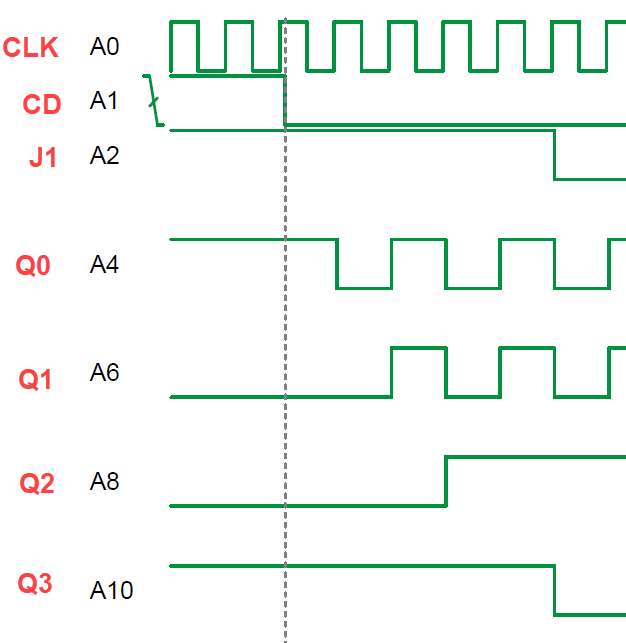
Print and discuss results from the logic analyser. When printing and before handwritten annotations on the waveforms, change the Proteus logic analyser colour scheme to white and remove (blank) the generic grid and the unused channels. Add your own vertical time lines of interest to explain how the circuit behaves.
 |
|
Fig 3. Example of clean waveforms from the Proteus logic analiser printing before annotating comments. Add your vertical time lines of interest. |
Project location:
C:\CSD\P5\Circuit_C\proteus\(files)
Method III: using VHDL EDA synthesis and simulation tools (plan C2 circuit).
Get the component JK_FF model and translate to VHDL the top circuit (Circuit_C.vhd) to be able to start a new multiple-file plan C2 project.
CPLD or FPGA target chip options:
option #1.: MAX II
option #3.: Cyclone IV
Synthesise the project and print the RTL view. Be aware that the "number of registers" in the project's summary spreadsheet must be correct.
Use a VHDL test bench to demonstrate that the timing diagram looks like that obtained in the previous analysis methods.
How can you observe and measure glitches, false states and complications around CLK transitions?
Project location:
C:\CSD\P5\Circuit_C\VHDL\(files)
| Home Term 24/25-Q1 Contact Products Electronic devices and companies Software Books Magazines Instruments DEE Library EETAC DEEL |

|
|
| Web activa des de 09/2001, @ F. J. Robert, J. Jordana. Web editat amb Microsoft Expression Web 4. El contingut és un complement als materials d'estudi del curs Circuits i Sistemes Digitals disponibles al campus digital Atenea. Llicència:Reconeixement 4.0 Internacional de Creative Commons |