|
|
Bachelor's Degree in Telecommunications Systems and in Network Engineering |
|
|
Hex_7seg_decoder plan C2 using method of memories |
P2 |
Method of memories for implementing logic functions
| 1. Specifications | Planning | Developing | Functional test | Gate-level test | Prototype | Report |
Design a hexadecimal to 7-segment decoder using plan C2 and memory chip components.
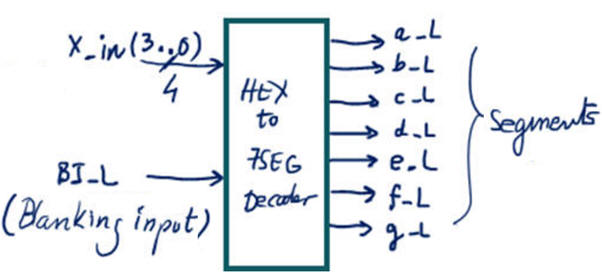 |
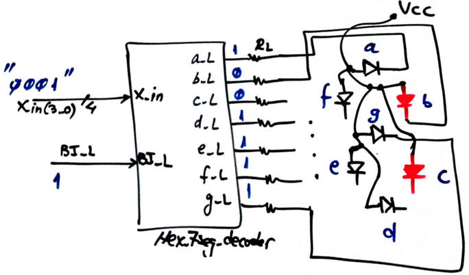
| Fig. 1. Hexadecimal to 7-segment decoder. A similar standard chip is the 74LS47. |
When BI_L is active with a low level ('0') all outputs are high ('1'), meaning that no LED is lighting (blanked).
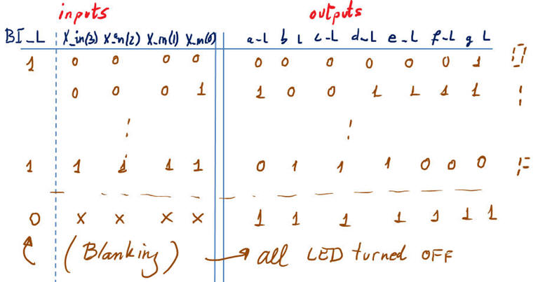 |
| Fig. 2. This is the truth table to define how the circuit works and that always goes attached to the symbol. |
Example of a timing diagram. Plan some input vectors and figure out which are going to be the outputs.
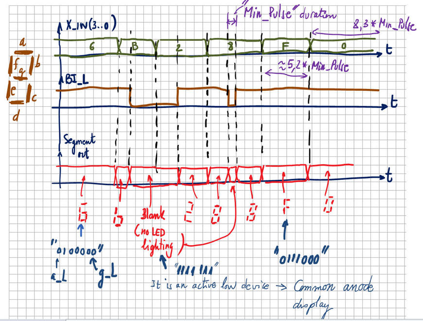 |
| Fig. 3. The sketch of the timing diagram that is expected from this circuit. |
| Specifications | 2. Planning | Development | Functional test | Gate-level test | Prototype | Report |
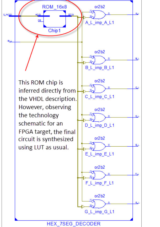
We will conceive all our circuits using VHDL EDA tools and following the design flow. Fig. 3 shows the internal architecture of the circuit. Fig. 4 shows the plan using a ROM16x8 component and logic gates.
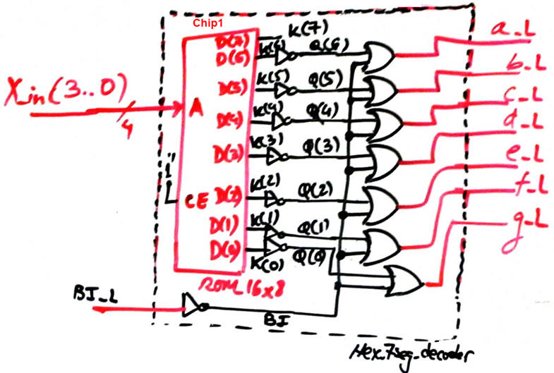 |
| Fig. 4. Plan proposed for this project. |
Demonstration on how the truth table is generated for a given input combination.
 |
| Fig. 5. Normal decoding with active-low outputs is done when BI_L is disabled. |
Project location:
C:\CSD\P5\Hex_7seg_decoder\(files)
| Specifications | Planning | 3. Development | Functional test | Gate-level test | Prototype | Report |
This "Hex_7seg_decoder.vhd" is the translation of the circuit in Fig. 4 above.
The components have their own translation to VHDL, for instance: "ROM_16x8.vhd" adapting files from this ROM unit.
Implement a new synthesis project using Quartus Prime for a given Intel target chip: FPGA Cyclone IV EP4CE115F29C7.
Print and discuss RTL and technology circuits.
 |
| Fig. 6. RTL circuit. |
How many chip resources (logic cells) are used?
| Fig. 7. Technology circuit. |
| Specifications | Planning | Developing | 4. Functional test | Gate-level test | Prototype | Report |
Draw a testbench fixture. We will simulate in ModelSim a VHDL testbench for the unit-under-test.
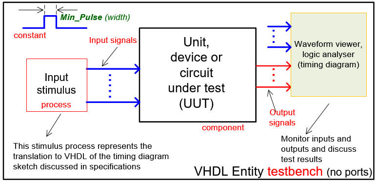 |
| Fig. 8. Testbench VHDL fixture schematic for performing functional and gate-level tests. |
The testbench is the same as in P2 using plan A or Hex_7seg_decoder using plan B.
| Specifications | Planning | Developing | Functional test | 5. Gate-level test | Prototype | Report |
| Specifications | Planning | Developing | Functional test | Gate-level test | 6. Prototype | Report |
| Specifications | Planning | Developing | Functional test | Gate-level test | Prototype | 7. Report |
Follow this rubric for writing reports.
| Home Term 26/27-Q1 Contact Products Electronic devices and companies Software Books Magazines Instruments DEE Library EETAC DEEL |

|
|
| Web activa des de 09/2001, @ F. J. Robert, Web editat amb Microsoft Expression Web 4. El contingut és un complement als materials d'estudi del curs Circuits i Sistemes Digitals disponibles al campus digital Atenea. Llicència:Reconeixement 4.0 Internacional de Creative Commons |