|
|
Bachelor's Degree in Telecommunications Systems and in Network Engineering |
|
|
|
||
|
|
MUX_8: hierarchical structural single-file VHDL (plan C1) |
|
|
|
||
Optional supplemental resources
1. Specifications
Design a MUX_8 type 74HCT151 using plan C1.
|
|
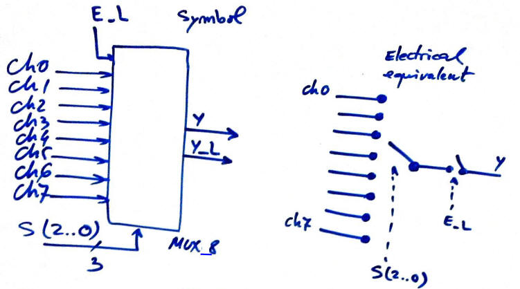
| Fig. 1. MUX_8 symbol |
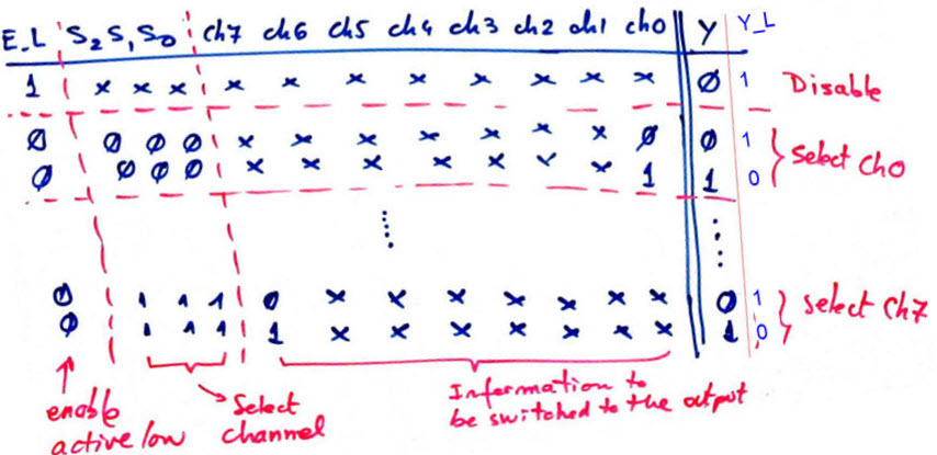
In Fig. 2 is represented the circuit's truth table.
|
|
| Fig. 2. Truth table. |
Finally, in Fig. 3 there is an sketch of a timing diagram.
|
|
|
Fig. 3. Example of a timing diagram sketch timing diagram to demonstrate how the circuit works for different inputs and so, be able to translate it later to VHDL as a testbench. |

2. Planning
|
Plan C1: hierarchical structure in a single file connecting smaller devices of the same kind and other circuits or logic. |
|
1.- Invent an internal architecture composed of several building blocs interconnected together. Analyse Fig. 4, this is the implementation of a MUX_8 using a hierarchical approach composed of a network of components of the same kind and other devices or logic in a single VHDL file (flat). 2.- Use a VHDL description of every block (equations/truth tables or algorithms, etc.) connecting them using signals. 3.- Find a similar VHDL circuit with a similar structural architecture to copy and adapt. 4.- Save files and develop and test the project at this location: C:\CSD\P2\MUX_8C1\(files) |
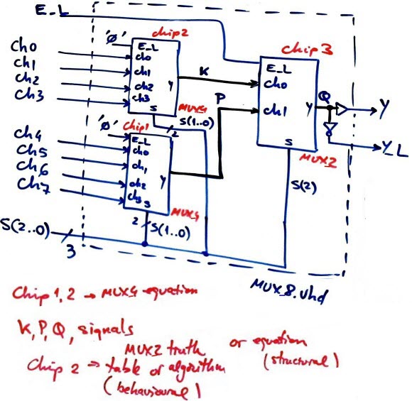 |
Fig. 4. Multiplexer expansion idea. This is an architecture proposed for the MUX_8 organised as a hierarchical design containing components of the same kind (MUX_2, etc., logic gates and wires (signals):
|
3. Development
1.- Write VHDL files. The entity name is related to the symbol in Fig. 1. Note that in this project channel inputs are not considered a vector but individual wires.
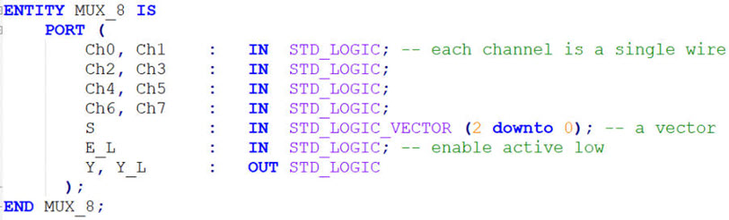 |
| Fig. 5. Entity description of the entity is the same for all design plans. |
This is single flat file MUX_8.vhd translating the architecture shown in Fig. 4.
|
|
2.- Synthesise the circuit's architecture accordingly to the plan C1 for a given target FPGA:
Start an EDA tool project for a sPLD/CPLD/FPGA chip MUX_8_prj and obtain the synthesised circuit. It is a project consisting of a single VHDL file (flat design).
Print, analyse and comment the computer generated RTL and technology views or schematics of the circuits.
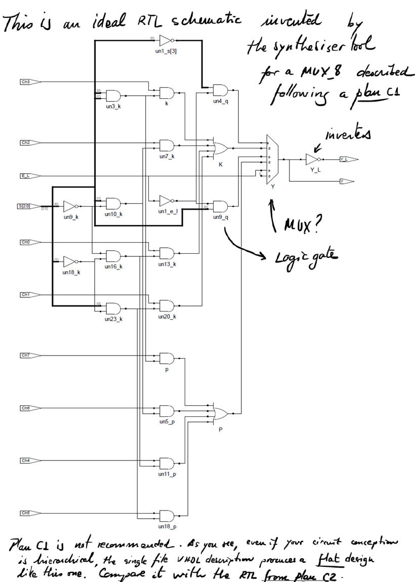 |
| Fig. 6. Example of RTL. |
 |
| Fig. 7. Example of technology view. |
Discuss the advantages and drawbacks of each development. Compare specifically the RTL and technology views of the three methodologies.
4. Testing
To test the solution whatever the plan used for designing its architecture, use the same test bench; the entity does not change. The testbench fixture containing the main ideas and concepts involved in this schematic is represented in Fig. 9.
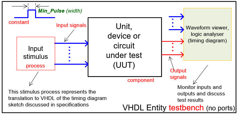 |
| Fig. 8. Testbench VHDL schematic. |
1.- Generate the template of the VHDL simulation testbench. The name of the file will be: MUX_8_tb.vhd (if the tool generates a MUX_8.vht, simply rename and copy it at project folder).
2.- Start an EDA VHDL simulator project to verify the Device-Under-Test (DUT) using a VHDL simulator test bench.
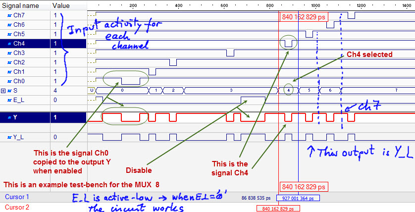
This is an example of testbench MUX_8_tb.vhd where inputs have been stimulated with logic values. Copy and paste to your design only constant Min_Pulse and input signals stimulus process. Testbench VHDL simulation stimulus is the translation to VHDL of the timing diagram in Fig. 3.
3.- Start the simulation process with only a few input vectors (from the timing diagram sketch in the specifications) to see if the whole simulation process works and you are able to watch correctly input and output signals activity.
4.- Verify applying sufficient test vector that the device works as expected (verify how the information of each channel is selected). Print the timing diagram screen and add comments on the signals to show how the device works.
In Fig. 9 there is an example of commented test bench results from the logic analyser (wave) available in the EDA tool simulation tool. Use coloured pens.
 |
|
Fig. 9. Example of a timing diagram produced by the simulator with some mandatory comments and discussion on the way the circuit works. |
5. Report
6. Prototyping
An example of laboratory prototype for testing multiplexers is presented in LAB2.
| Home Term 26/27-Q1 Contact Products Electronic devices and companies Software Books Magazines Instruments DEE Library EETAC DEEL |

|
|
| Web activa des de 09/2001, @ F. J. Robert, Web editat amb Microsoft Expression Web 4. El contingut és un complement als materials d'estudi del curs Circuits i Sistemes Digitals disponibles al campus digital Atenea. Llicència:Reconeixement 4.0 Internacional de Creative Commons |