|
|
Bachelor's Degree in Telecommunications Systems and in Network Engineering |
|
|
|
||
|
|
MUX_8: hierarchical structural multiple-file VHDL (plan C2) |
|
|
|
||
Type 74HCT151 commercial chip
1. Specifications
Let's design a MUX_8 using plan C2 based on components and signals. This is a hierarchical structure composed of multiple VHDL files rec. The circuit's symbol and truth table is discussed in Fig. 1 and naturally they are the same that were discussed in plans A or B.
|
|
| Fig. 1. Symbol and truth table. |
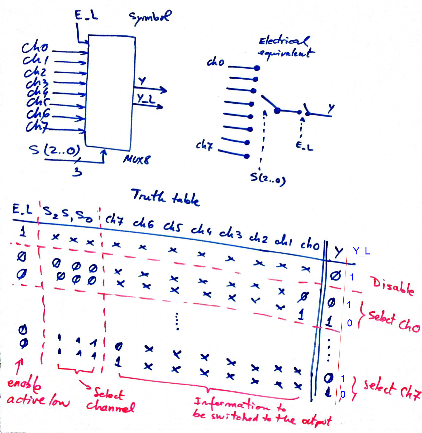
Fig. 2 shows an example timing diagram, so that you can predict which is the output for a given set of input vectors in time. When verifying the design in a VHDL test bench, the inputs from this sketch will be translated to the VHDL syntax, and the simulator will calculate the outputs. The output Y_L = Y'.
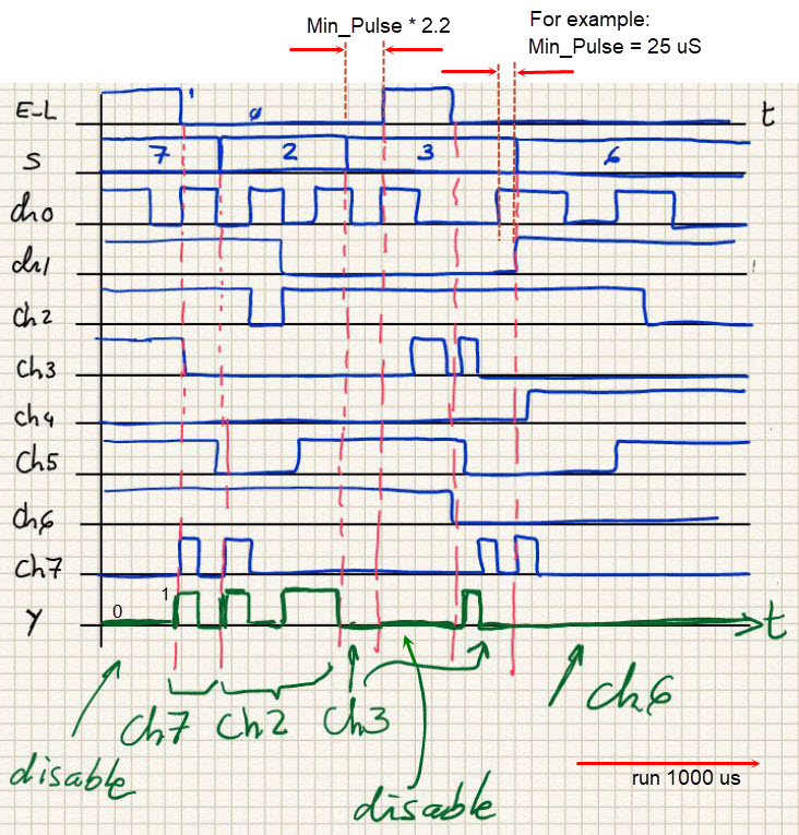 |
Fig. 2. A timing diagram sketch. |
2. Planning
Let's organise the following internal architecture in Fig. 3 based on using smaller components of the same kind and extra logic gates if necessary. This is the project location:
<disk>/CSD/P3/MUX_8/(files)
This project will consist of 3 VHDL source files. As you see, the components themselves are other projects, which have to be solved previously, so that you can use here only the verified MUX_4.vhd and MUX_2.vhd source files.
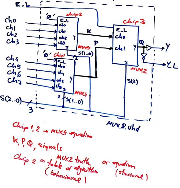 |
Fig. 3. The proposed plan, were every chip and wire must be annotated. This approach is an answer to the question: "How to expand it?" in our concept map. It is the same for decoders, multiplexers, encoders, etc. For instance: how to build a Dec_4_16 using Dec2_4 components?
Note: This rec presents a similar multiple-file structure showing that inventing circuits is all about creativity. Translate it to VHDL as yet another version of the top MUX_8.vhd. |
3. Developing the project using EDA tools
The translation of the plan in Fig. 2 generates the VHDL file corresponding to the top circuit mux_8.vhd,. The components themselves have their own translation to VHDL, for instance: mux_4.vhd (using plan A) adapted from this MUX_8 tutorial in Lab2), mux_2.vhd (using plan B adapted from this tutorial in Lab2).
Run a new EDA project MUX_8_prj including all the VHDL files to synthesise the circuit. In Fig. 3 there is a representation of the RTL schematic.
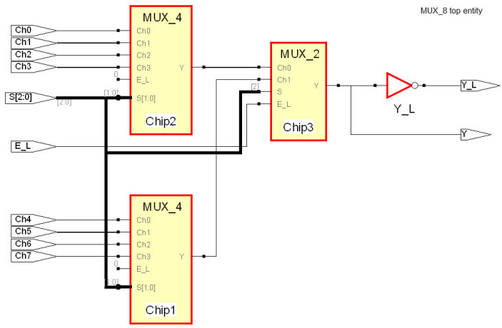 |
Fig. 3. The RTL circuit generated by the EDA synthesiser.
Note: |
In case you like to design all the components identically, for instance, this is a mux_2.vhd that has an additional Y_L output, and so it looks now like the little brother of the MUX_8.
4. Testing and validating the design - Functional Simulation
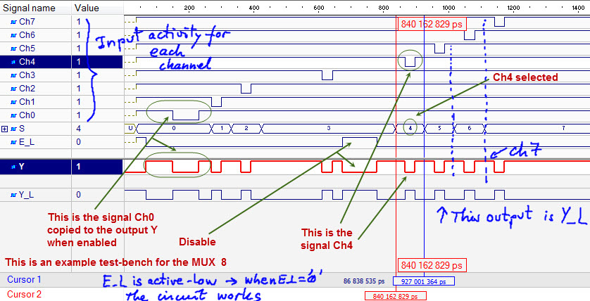
From an initial VHDL test bench MUX_8_tb.vhd, run the VHDL simulation EDA tool to obtain and discuss the timing diagram. This below in Fig. 4 is an example of resulting waveforms.
 |
|
Fig. 4. The test results from the VHDL simulator that verifies the circuit's operation. |
5. Testing and validating the design. Gate-level and timing analyser
The gate-level simulation and the timing analyser is from P4. This is a video rec discussing the question: How fast is the circuit when implemented in a Cyclone IV FPGA? The answer is calculated to be 100 MHz, meaning 100 million operations of multiplexing data per second.
6. Report
Project report starting with the template sheets of paper, scanned figures, file listings, docx , pptx, or any other resources. Every printed documents has to have pen annotations with explanations and discussion.
7. Prototyping
Use the training board in the lab that contains the project target chip and perform laboratory measurements to verify how the design works.
| Home Term 26/27-Q1 Contact Products Electronic devices and companies Software Books Magazines Instruments DEE Library EETAC DEEL |

|
|
| Web activa des de 09/2001, @ F. J. Robert, Web editat amb Microsoft Expression Web 4. El contingut és un complement als materials d'estudi del curs Circuits i Sistemes Digitals disponibles al campus digital Atenea. Llicència:Reconeixement 4.0 Internacional de Creative Commons |