|
|
Bachelor's Degree in Telecommunications Systems and in Network Engineering |
|
|
|
Design Circuit_K using plan A |
Circuit_K plan B |
Circuit_K plan C2 |
| A1: PoS | A2: only NAND_2 |
| 1. Specifications | Planning | Developing | Testing | Report | Prototype |
Implement the truth table written in Fig. 1 using plan A and the minimised equation product of sums (PoS) from minilog.exe. Check your solution using VHDL tools.
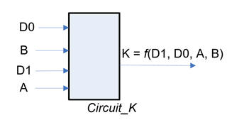 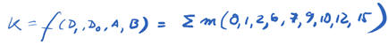 |
| Fig. 1. Circuit_K to desing. K = f(D1, D0, A, B) |
| Specifications | 2. Planning | Developing | Testing | Report | Prototype |
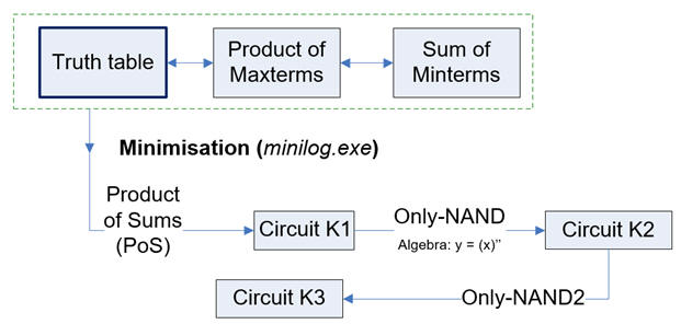
From the initial specifications in Fig. 1 you can invent/create/infer and test/check/verify several circuits as shown in L1.4.
 |
|
Fig. 2. Designing two circuits from the same initial truth table. |
Concepts about transforming circuits to contain only NAND are explained in lecture L1.5.
Project location:
C:\CSD\P1\Circuit_K\PoS\(files)
| Specifications | Planning | 3. Developing | Testing | Report | Prototype |
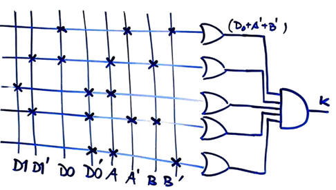
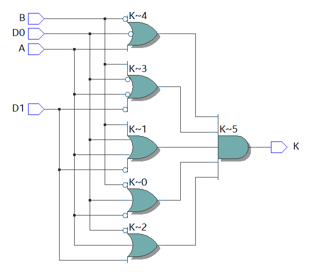
Using minilog with Circuit_K.tbl the Circuit_K1 based on PoS can be obtained:
  |
|
Fig. 3. Circuit_K1 PoS equation from minilog. |
| Specifications | Planning | Developing | 4. Testing | Report | Prototype |
Testing means to check or verify that the solution is correct and agrees with the initial specifications. Circuit_K1 based on PoS can be checked using a VHDL project from the architecture in Fig. 3 translated as Circuit_K1.vhd.
 |
|
Fig. 4. Circuit_K1 RTL schematic showing the PoS circuit. |
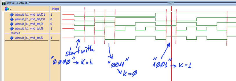
Using a testbench fixture Circuit_K1_vhd.vhd we can test the solution.
 |
|
Fig. 5.Truth table verification using a VHDL testbench . |
| Specifications | Planning | Developing | Testing | 5. Report | Prototype |
Follow this rubric for writing reports.
| Specifications | Planning | Developing | Testing | Report | 6. Prototype |
We can use the DE10-Lite board to implement this project, as shown in Lab 1.2 for the similar Circuit_W.
| A1: PoS | A2: only NAND_2 |
| 1. Specifications | Planning | Developing | Testing | Report | Prototype |
Implement the truth table written in Fig. 1 using plan A from the previous SoP and using only 2-input NAND gates. Check the solution using Proteus.
|
|
|
Fig. 1. Circuit_K to desing. K = f(D1, D0, A, B) |
| Specifications | 2. Planning | Developing | Testing | Report | Prototype |
We can transform the SoP equation from the previous design. Concepts about transforming circuits to contain only NAND are explained in lecture L1.5.
 |
|
Fig. 2. Designing two circuits from the same initial truth table. |
Project location:
C:\CSD\P1\Circuit_K\NAND_2\(files)
| Specifications | Planning | 3. Developing | Testing | Report | Prototype |
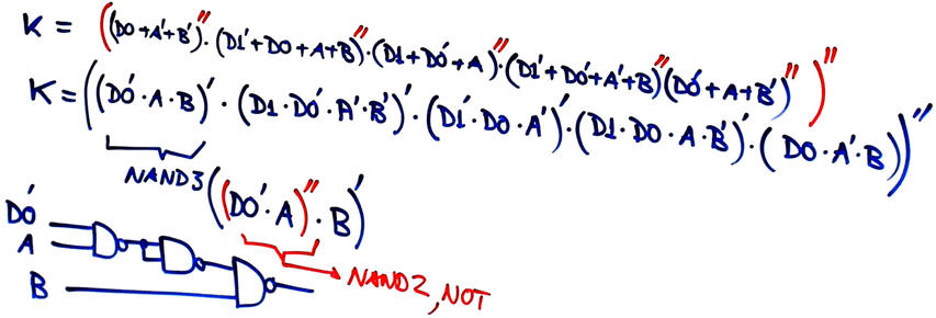
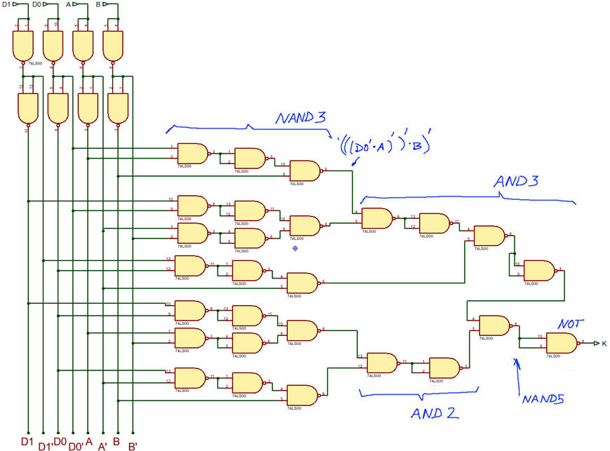
And modifying Circuit_K1 we can deduce Circuit_K3 in two steps: 1) circuit based on only-NAND; 2) transform all NAND gates to NAND2.
  |
|
Fig. 3. Circuit_K2 schematic consisting of only NAND. And the required transformation of each NAND so it can be implemented using only NAND2 chips. |
| Specifications | Planning | Developing | 4. Testing | Report | Prototype |
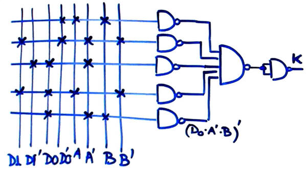
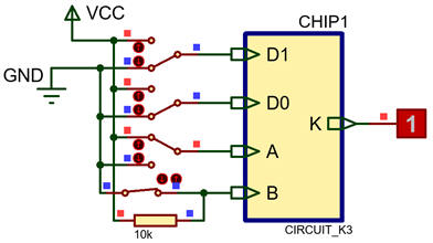
Circuit_K2 using only NAND (Circuit_K2_equ.txt) checked using WolframAlpha (Method IV) do not work because the equation is too long. Thus, the alternative is to use Proteus (method II and a given library of components such 74LS-TTL): Circuit_K3.pdsprj or VHDL (method III).
  |
|
Fig. 4. Circuit_K3 captured in Proteus for truth table verification. This picture shows how input "0010" generates the m2. |
| Specifications | Planning | Developing | Testing | 5. Report | Prototype |
Follow this rubric for writing reports.
| Specifications | Planning | Developing | Testing | Report | 6. Prototype |
We can use the DE10-Lite board to implement this project, as shown in Lab 1.2 for the similar Circuit_W.
| Home Term 26/27-Q1 Contact Products Electronic devices and companies Software Books Magazines Instruments DEE Library EETAC DEEL |

|
|
| Web activa des de 09/2001, @ F. J. Robert, Web editat amb Microsoft Expression Web 4. El contingut és un complement als materials d'estudi del curs Circuits i Sistemes Digitals disponibles al campus digital Atenea. Llicència:Reconeixement 4.0 Internacional de Creative Commons |