|
|
Bachelor's Degree in Telecommunications Systems and in Network Engineering. Bachelor's Degree in Aerospace Systems Engineering |
|
|
Power lamp PWM control using a PIC µC |
Phase #1 |
Initial remark: We can program a C language application for PIC18F microcontrollers considering two coding styles or design patterns for control flow:
(A) BM: Bare-metal as in CSD Chapter 3, direct register-level configuration of the PIC system and peripherals. This is basic summary of the PWM peripheral module. This style is recommended for discovering the basic parameters of this peripheral.
(B) MPLAB Code Configurator (MCC Melody). This is the recommended way for professional applications. We propose to solve the project using this style.
| 1. Specifications | Planning | Developing & testing | Prototype | Report |
Project page for the dimmer's Option #B2: µC design. Let us use the CSD_PICstick board to provide a digital control of the lamp, as if this project were the CSD D3.5 version V2. We will use the PWM peripheral.
Design phase #1:
-
MCC Melody programming.
-
10-bit pulse width (PW) adjustment. It means a duty cycle resolution of 0.1% from 0% to 100%. Let us select in this initial phase between two DC values using the board's switch SW1, for instance 35.3% and 83.6%.
-
10-bit wave period (WP) adjustment. In this initial phase let us fix this parameter to be a constant to generate fPWM_out = 2 kHz.
-
As for many other machines, let us start and stop (ST) the PWM generation using the board's PB1 push-button.
-
Let us verify the design using Proteus virtual laboratory simulations and on the CSD_PICstick prototype.
Design phase #2:
-
Let us add the LCD display to the system to show information on the waveform parameters.
Design phase #3:
-
Let us add the PWU and PWD push-buttons to fix the pulse duration. Or, alternatively, a digital rotary encoder or an analogue potentiometer.
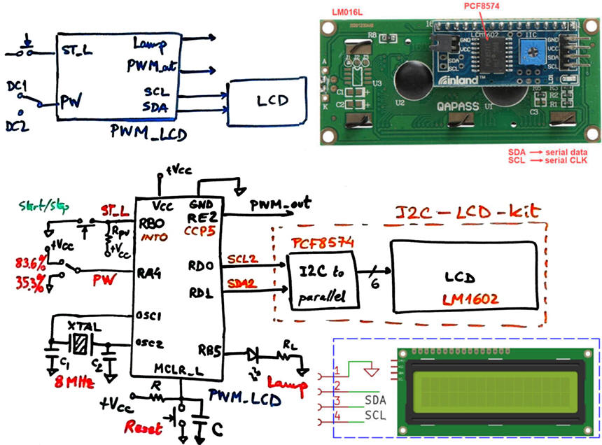
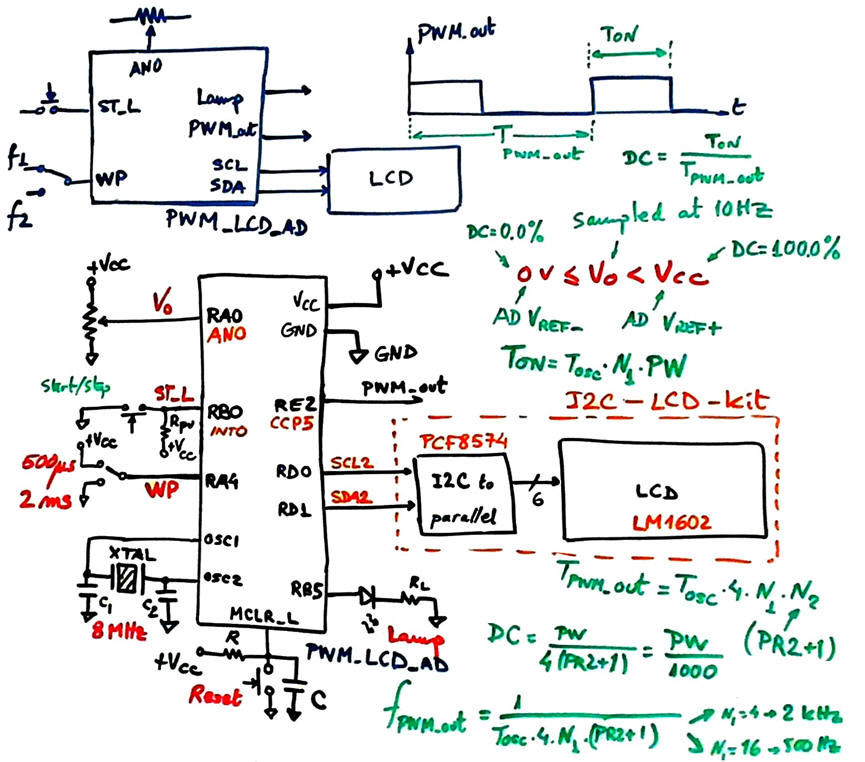
This PWM units explains the parameters controlling the generated waveform.
PW and WP parameters are linked, and thus the frequency of the waveform and the duty cycle (DC) resolution. For instance, WP = 1000 (10-bit), allows 0.1% resolution or up to 1000 DC increments. If we fix WP = 100 (7-bit) we obtain 1% DC resolution (100 steps).
Furthermore, the PWM peripheral architecture and the 8 MHz µC oscillator crystal determines the maximum frequency generated for a given DC resolution. For example, if 0.1% DC resolution is required (10-bit, 1000 DC levels), TMR2 has to count up to one thousand every period (N1·N2 = 1000): fPWM_outmax < 2 kHz. However, if only 6.25% DC resolution is required (4-bit, 16 DC levels): fPWM_outmax < 125 kHz.
For our LED lamp control, the signal frequency has to be high enough for the eye not to perceive the flicker. Register values allow only some frequencies. For instance, for 0.1% DC resolution we can generate fPWM_out = 2 kHz using TMR2 prescaler = N1 = 4 and PR2 = N2 = 249). Likewise, we can generate fPWM_out = 500 Hz using TMR2 prescaler N1 = 16 and PR2 = N2 = 249).
|
|
|
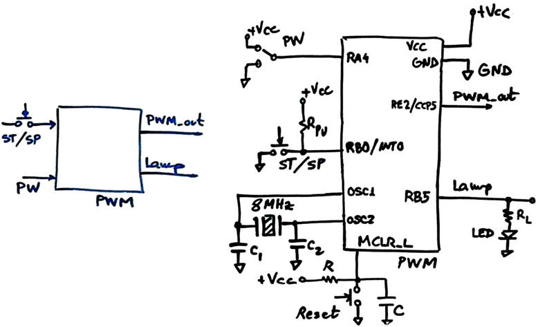
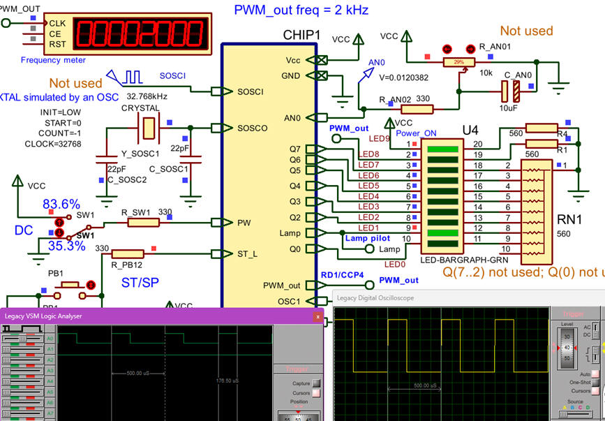
Fig. 2. Symbol and the main components on PWM generation. |
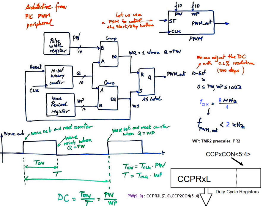
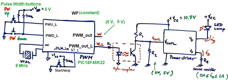
Fig. 3 shows how the PWM_top drives the optocouple and the lamp.
|
|
|
Fig. 3. PWM_top circuit for controlling the light intensity of the LED lamp. The PWM waveform is connected to the power driver using a phototransistor coupler adapting control voltage levels at the same time. |
| Specifications | 2. Planning | Developing & testing | Prototype | Report |
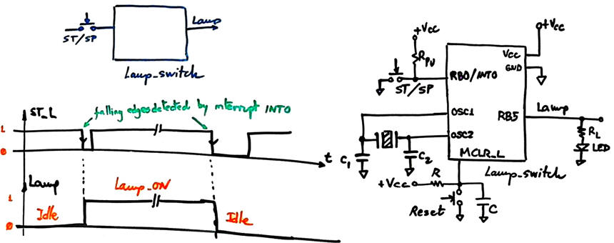
Design phase #1: As shown in Fig. 4, we can start drawing the symbol for the basic PWM circuit. The FSM will drive PWM_out and control external start/stop pulses ST.
To make it easier, two steps may be considered:
-
Step #1: Lamp ON/OFF to install the FSM and the external interrupt. Let us adapt de blinking LED project from the MCC unit.
 |
|
Fig. 4. Symbol and electronic schematic for the lamp switch. |
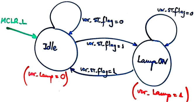
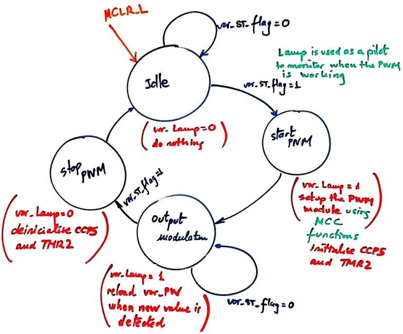
Fig. 5 presents the state diagram for the FSM consisting of only two states.
|
|
Fig. 5. State diagram. |
Project location:
C:\DEE\Dimmer\PIC\PWM1\(files)
-
Step #2: Replace the lamp switch by the lamp PWM control.
Let us in this phase to select between two duty cycle values using the board's switch SW1, for instance DC1 = 35.3% and DC2 = 83.6%.
|
|
Fig. 6. Symbol and schematic. |
Two new states are used to setup and switch off the PWM peripheral.
|
|
Fig. 7. State diagram that starts and stops the PWM peripheral. All functions used to drive the module are generated and maintained by MCC. |
Project location:
C:\DEE\Dimmer\PIC\PWM2\(files)
| Specifications | Planning | 3. Developing & testing | Prototype | Report |
Step #1: Lamp ON/OFF to install the FSM and the external interrupt.
To copy and adapt our tutorial we follow this sequence:
-
Get the tutorial example Blink_LED_FSM from the MCC unit, compile and check that it works as expected using Proteus. This step is for checking your MPLABX, XC8 and Proteus tools.
-
Move the project to the new location "C:\DEE\Dimmer\PIC\PWM1".
-
Rename the project as "Lamp_switch_prj" including the project folder
-
Remove the main C source file from the project and add the new "Lamp_switch.c"
-
Edit its #include "./Lamp_switch_prj.X/mcc_generated_files/system/system.h"
-
Rename the important file "Lamp_switch_prj.mc3"
-
Compile to generate the new "COF"
-
Rename the Proteus subcircuit to be LAMP_SWITCH
-
Attach the new "COF" to the µC and run to check that everything works as expected.
This is the zipped project: "Lamp_switch.zip". We can take and adapt it for the next step.
Step #2: Basic PWM with a switch to select between two PW values.
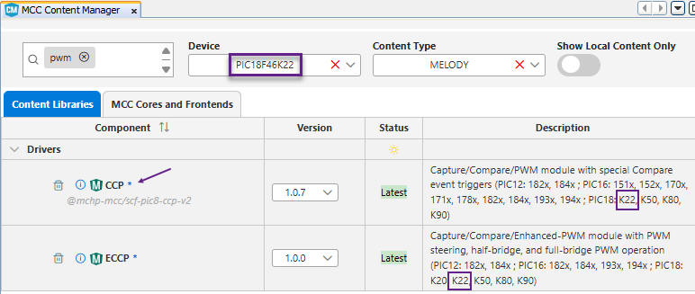
We explore the MCC Content Manager to filter which drivers to use when configuring the hardware in the MCC for the PIC18F46K22 device:
|
|
Fig. 8. We can search through the MCC content manager which components for the PIC18F46K22 to add to our project. |
|
|
Fig. 9. We can search through the MCC content manager which components for the PIC18F46K22 to add to our project. |
And again, we rely in our tutorial examples to adapt this project.
This is the zipped project: "PWM.zip". We can take and adapt it for the next step.
|
|
Fig. 10. We run Proteus to debug the system and save muh of lab prototyping time. We will proceed with prototyping only when the system is already operating correctly in the virtual laboratory. |
| Specifications | Planning | Developing & testing | 4. Prototype | Report |
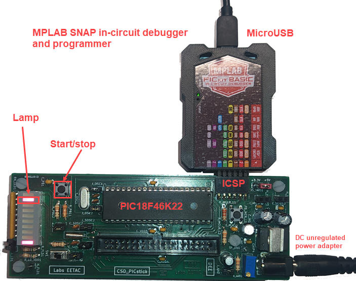
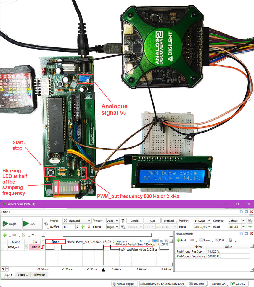
Step #1: Let us upload the program to the PIC18F46K22 and watch the signals using laboratory instrumentation. We can also use the MPLAB SNAP in-circuit debugger as we did in Proteus to watch run time RAM variables.
|
|
Fig. 11. CSD_PICstick board running the step #1 lamp switch. |
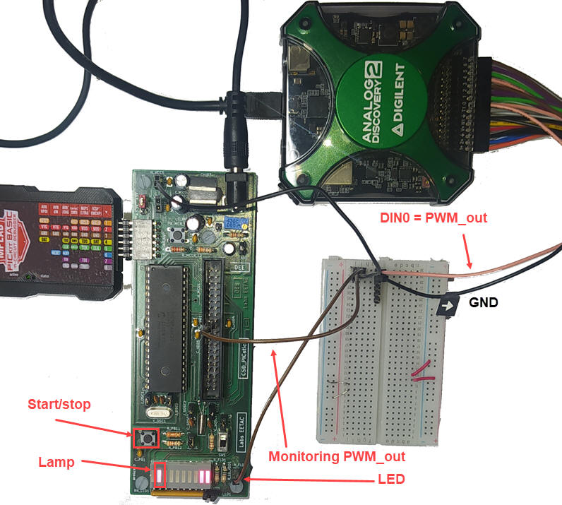
Step #2: PWM with a switch to select between two PW values.
|
|
Fig. 12. CSD_PICstick board running the step #2 PWM application. PWM_out is monitored using the logic analyser DIN0 or the oscilloscope CH1. |
|
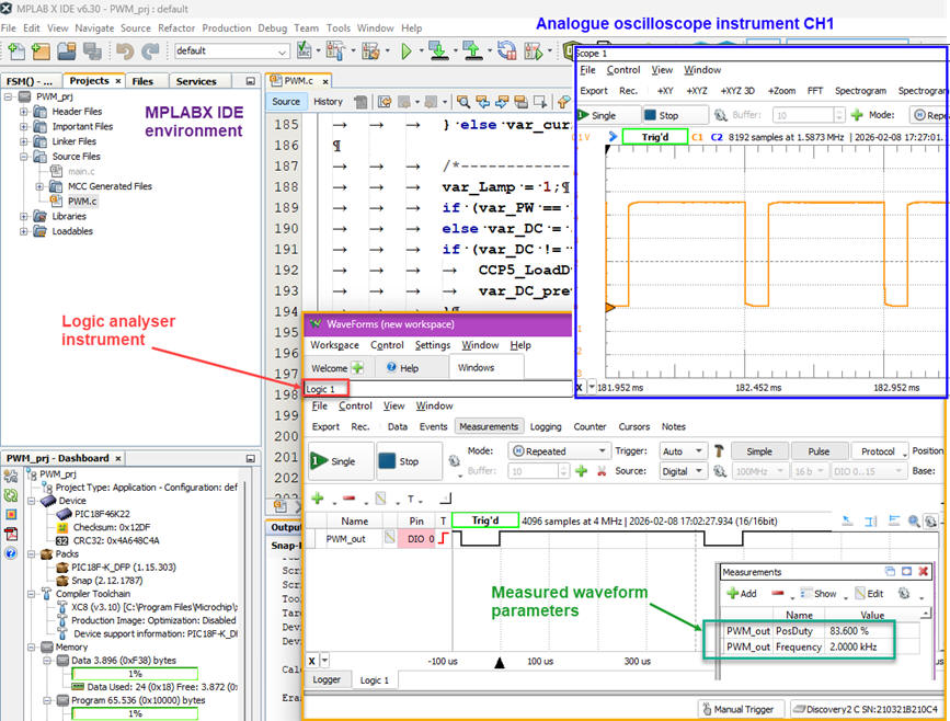
|
Fig. 13. Waveform measurements using the Analog Discovery 2 from Digilent. |
| Specifications | Planning | Developing & testing | Prototyping | Report |
As you can see, the purpose of these pages is to show you examples on how to organise professional reports. Your aim is to design systematically, enhancing your product step by step. And, at the same time, publish quality technical materials and slides for public presentations. At this stage, you can continue enhancing your product adding new features.
|
Power lamp PWM control using a PIC µC |
Phase #2 |
Design phase #2: PWM circuit with LCD display
Specifications
-
Add the I2C LCD kit to the PWM control to write ASCII messages.
|
|
Fig. 1. Symbol and schematic. Interfacing the LCD with only two wires will simplify the hardware interface, specially when other sensors and actuators may be connected to the same I2C bus. |
Planning
We will copy the phase #1 project to the new location and adapt the I2C LCD library from the MCC example (tutorial 7, annex 3).
Project location:
C:\DEE\Dimmer\PWM_LCD\(files)
Development and test
Let us start repeating the sequence for not starting from scratch but copying and adapting the last phase #1 step #2. on the new location.
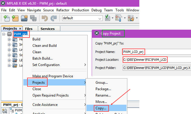
1) Open the last phase #1 step #2 project "PWM_prj" in the MPLABX IDE.
2) Copy the current "PWM_prj" project to the new "PWM_LCD_prj":
|
|
Fig. 2. Copy he project to the new location. |
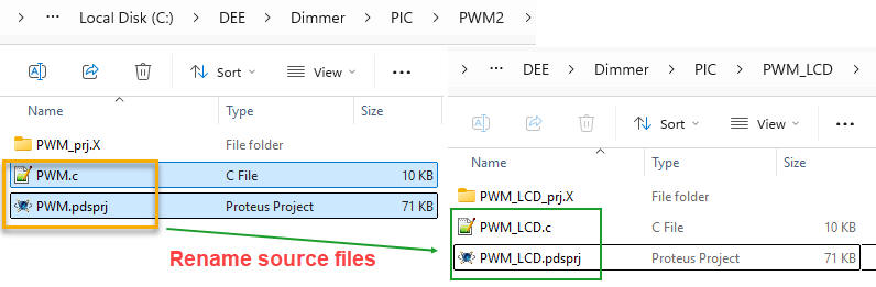
3) Copy and rename our hardware and software source files at the new location:
|
|
Fig. 3. Rename the source files and add the new ones. |
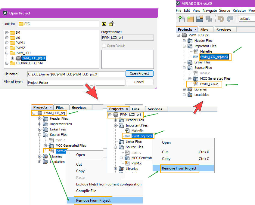
4) Open the new project and remove the old source files and also the important file "PWM_prj.mc3":
|
|
Fig. 4. Remove the old source files in the new project, and add the new ones. |
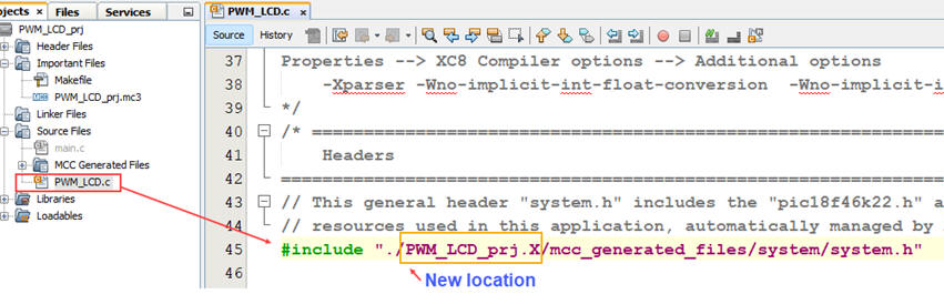
5) Edit the source file "PWM_LCD.c" to update the location for the "system.h" include.
|
|
Fig. 5. Edit the location of the MCC-generated hardware support. |
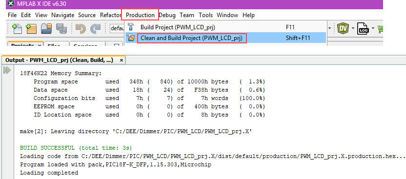
6) Compile and generate the new project to check that it has no errors.
|
|
Fig. 6. Compile. |
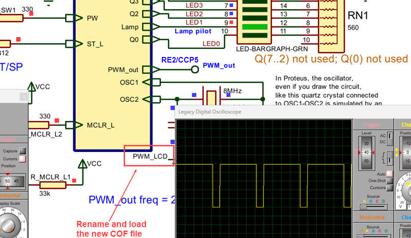
7) Update the circuit "PWM_LCD.pdsprj" and rename the subcircuit; load and attach the new "cof" to the µC; run to check that it works as expected.
|
|
Fig. 7. Run the simulation and check how it works. |
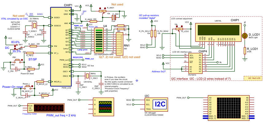
Hence, everything is ready to add the new hardware LCD kit and its software library. Our initial "Hello World" will be printed on the screen. This means that there is no errors in our hardware-software development environment. Once this initial step works, we can try to represent in text the two duty cycles selected with the SW1.
The Proteus environment for debugging and making measurements.
|
|
Fig. 8. Edit the hardware circuit to include the new components. |
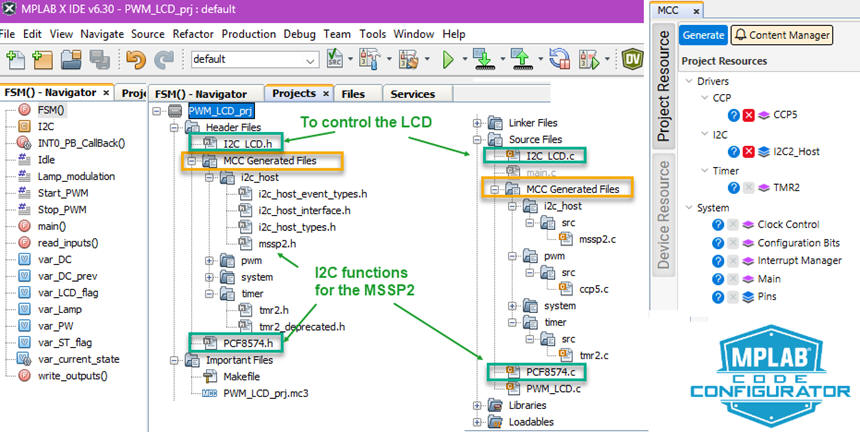
The MPLABX environment where the MCC Melody is used to drive and configure all the µC hardware resources .
|
|
Fig. 9. Add the I2C interface through the MCC tool. |
This is the zipped project: "PWM_LCD.zip". We can take it as the initial starting point for the next phase #3.
|
|
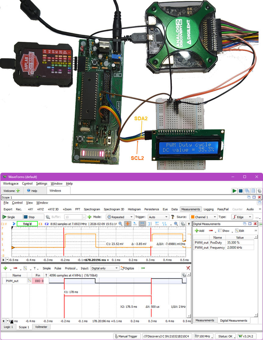
Fig. 10. Phase #2 prototype running. We can verify that the DC precision is 0.1% for the full range using the laboratory instrumentation. We can also use the in-circuit debugger to watch RAM variables or stop the program execution anywhere by means of breakpoints, as we currently do in Proteus. |
|
Power lamp PWM control using a PIC µC |
Phase #3 |
Design phase #3: Making easy setting the lamp duty cycle and waveforms frequency.
Specifications
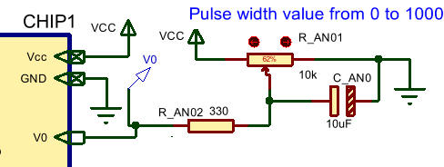
Add a potentiometer to obtain the pulse width PW using the 10-bit resolution A/D. The potentiometer voltage V0 is converted to the pulse width variable var_PW from 0% to 100% in 10 bit resolution. We can simply use the AN0 (RA0) pin to connect the potentiometer.
In this phase, we can use the switch SW1 to select between two waveform periods: WP1 = 500 µs, WP2 = 2 ms.
|
|
Fig. 1. Symbol and electronic circuit. |
Planning
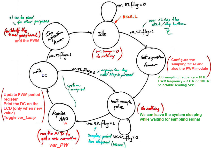
To build this system, we enhance the previous design phase #2 adapting the tutorial project FSM_AD_LEDbar that explains how to setup and run the A/D converter for a given sampling frequency fS. Therefore, Fig. 6 presents the state diagram for the FSM. At the state Set_acq_timer we will also configure the PWM module. The V0 acquired value will be for setting the duty cycle period register.
|
|
Fig. 1. State diagram adapted from the tutorial. The potentiometer is acquired at 10 Hz sampling frequency. |
Project location:
C:\DEE\Dimmer\PIC\PWM_LCD_AD\(files)
Development and test
Once again, let us repeat the same steps to start adapting the tutorial on the A/D to this system.
|
|
Fig. 3. The potentiometer to set the pulse duration value from 0 to 1000 using the 10-bit A/D converter is included in the CSD_PICstick. |
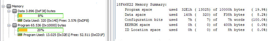
It is worth noting that for this simple application, where the free XC8 compiler is used, 20% of the program memory is occupied.
|
|
Fig. 4. Compiler results. |
This is the zipped project: "PWM_LCD_AD.zip".
Remember that following this indications, you can visualise on the watch window the var_DC floating point variable and its equivalent as ASCII text.
|
|
Fig. 5. Debugging dynamic data on the watch window and on the LCD. |
|
|
Fig. 5. The system running . |
The next step is to connect the PWM controller to the power LED lamp. We can add an optocouple to isolate the controller from the power driver.
Alternatively, we can replace the potentiometer adding two push-buttons to fix the duty cycle up and down PWU, PWD. For instance, at maximum resolution, let us sweep all PW values in 5 s using an internal 200 Hz CLK flag. Discuss which modules will this variation include.
| Home Contact Tutorials Electronic devices and companies Books Magazines Instruments Digsys Library EETAC DEEL |

|
|
| Web activa des de 01/2023, @ F. J. Robert. Web editat amb Microsoft Expression Web 4. El contingut és material de referència per al disseny d'equips electrònics. Llicència:Reconeixement 4.0 Internacional de Creative Commons |