|
|
Bachelor's Degree in Telecommunications Systems and in Network Engineering. Bachelor's Degree in Aerospace Systems Engineering |
|
|
|
Project: Power LED dimmer |
Project specifications |
Our goal is to design a dimmer to control the level of illumination or light intensity for a 10 W power LED.
|
|
|
Fig. 1. Commercial dimmer for power LED. |

Let us reuse and chaining previous content and projects. Let us imagine several design phases as if the circuit has to evolve adding new features and modules. For instance:
- Design phase A: Analogue system
A0.- The actuator: a commercial power LED. Heatsink. Bias point.
A1.- LED driver amplifier. Design equations. Modelling. Simulation. PWM driver using a 555 IC.
- Design phase B: Digital
FSM installation. ON (100% light intensity / OFF (0%, no light). Digital PWM. We can choose to use two UP/DOWN push-buttons or instead, a potentiometer to set the PWM duty cycle.
- Design phase C. Mains adapter and 12W switching power supply
- Design phase D. We can replace the control panel potentiometer or UP/DOWN buttons by a wireless control.
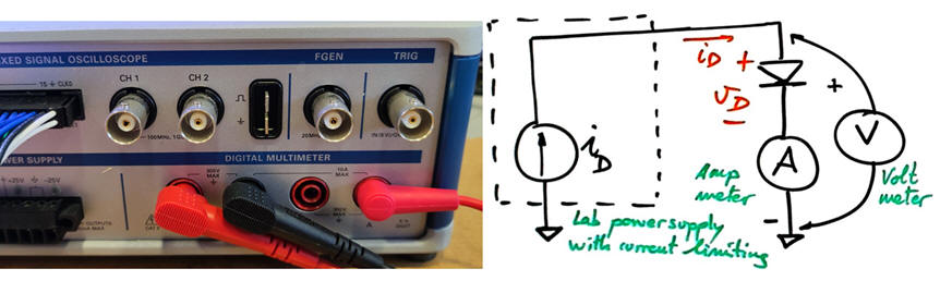
In phases A and B laboratory power supplies will be used as energy sources for driving circuits and the power LED.
References and additional questions
A good reference on what we are indenting to discuss in this introductory project can be read in subject CESA on [1] "Introducción al laboratorio: Dimmer", [2] "CESA: Ejemplos de actividades dirigidas".
|
|
Design phase A0: LED characteristics |
A0: LED characteristics |
|
|
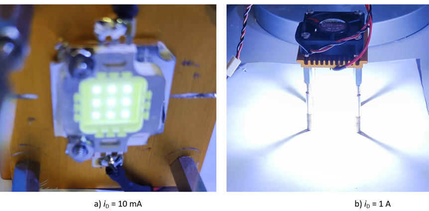
Characterise and experiment with a power LED lamp. Observe the maximum light intensity for a 10 W LED. Measure its forward current versus forward voltage function iD = f(VD).
A0.1 Power LED
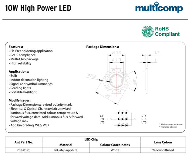
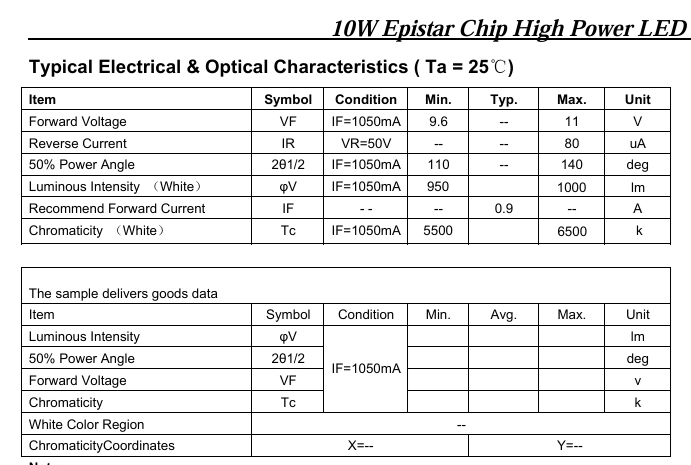
This actuator is an array of several LED connected in series and in parallel. Example datasheet from Epistar company.
|
|
Fig. 2. Typical power LED lamp. |
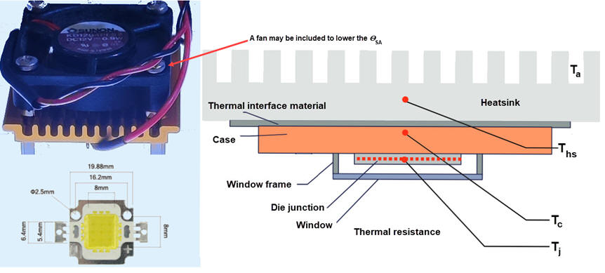
A0.2 Heatsink
This kind of actuators require designing a heatsink to keep the temperature in the specified range when working in nominal conditions. Therefore it has to be attached to a metallic heatsink and optionally to a fan even if it means an efficiency loss.
|
| Fig. 3. a) Fan, heatsink and LED lamp ready for experimentation. b) Thermal resistance electrical model. |
 a)
a)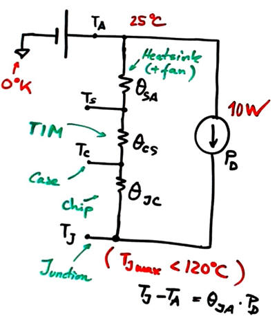 b)
b)Thermal resistance QTH calculations and temperature distribution at rated power.
A0.3 Characterisation
We need a laboratory power supply to observe how the LED works and which may be the correct bias point. We will validate the experiment checking datasheet data. We need to observe the light intensity generated by a single LED, in case we decide to connect several of them in the same luminary or panel.
|
|
|
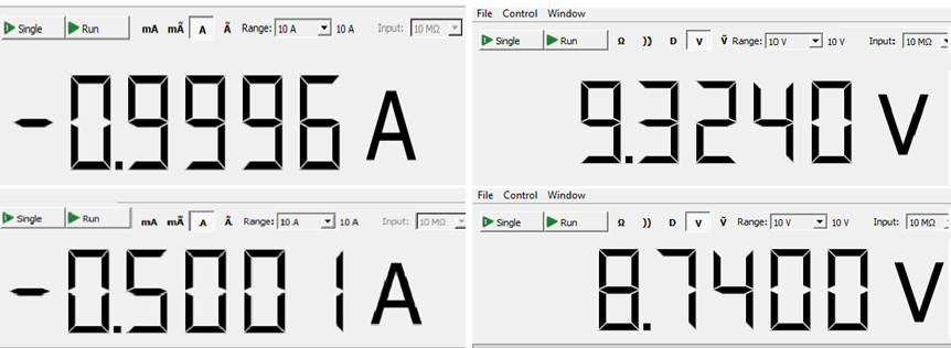
Fig. 4. Experiment for obtaining the function iD = f(VD) and two sample values at 0.5 A and 1 A. |
We can sweep the driving current iD from 1 mA to 1 A to annotate the measured diode voltage.
|
|
|
Fig. 4. Experimental iL = f(VD). curve characteristic. |
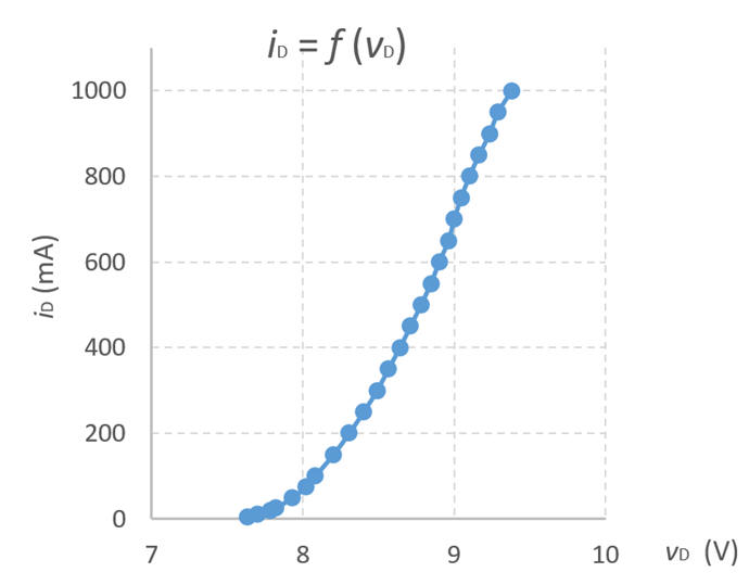
The exponential diode characteristic shows us that in order to obtain an effective analogue light intensity control from 0% to 100%, it will be much better to control the LED current iD than its voltage vD. Current margin from 1 mA to 1 A, voltage margin span from 7.5 V to 9.5 V. Therefore, we need a current source to drive the LED capable to adjust the required LED voltage.
|
|
Design phase A1: analogue control system |
1. A1 specifications |
To control the lamp light intensity we may propose two steps:
A1.1. Designing the LED lamp power driver
A1.2. Adding a PWM control signal
A1.1. LED lamp power driver
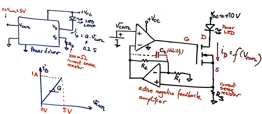
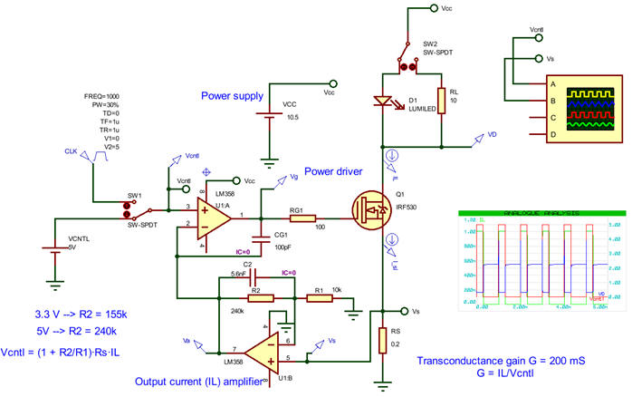
Let us propose a power driver for the LED. This device will be a transconductance amplifier, capable of controlling the output current iD proportionally to the much convenient input control voltage VCNTL. To adapt a circuit for our LED lamp we can examine the application note schematic reproduced in Fig. 1.
|
|
Fig. 1. Transconductance linear amplifier copied from the application note: Murnane, M., "AN-968: Current Sources: Options and Circuits", Analog Devices. |
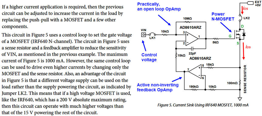
Instead of a simple jumper LK2 we will connect the floating LED lamp as the load. An active feedback path is used to sense the LED current iD while keeping a very low voltage VS.
|
|
Fig. 2. Transconductance linear amplifier. |
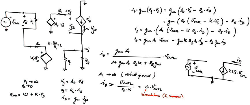
We can obtain circuit equations imagining virtual ground or very simple small-signal ideal OpAmps and components models as represented in Fig. 3.
|
|
Fig. 3. Small-signal low-frequency simplified schematic to deduce the design equation. |
It is interesting to analyse the circuit stability using simplified dominant-pole models for the components. Thus, capacitive compensation networks (C2) can be properly discussed along with PSPICE simulations in Proteus. Final prototypes and circuit measurements will also be required to assure that the system performs as expected.
Controlled current sources are typical OpAmp applications. Other materials and references:
[3] The LT1492 OpAmp datasheet from Analog Devices shows typical applications on power VCCS.
[4] Other references on controlling LED light intensity.
2. Planning
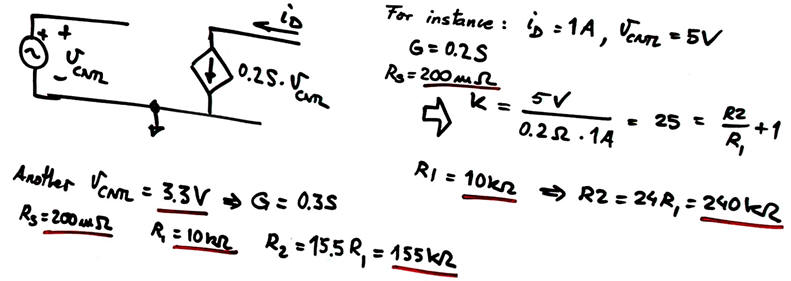
The proposed block diagram is shown in Fig. 2. It is based on using an OpAmp as high-gain linear amplifier. Example values are calculated in Fig. 4. The NMOS transistor will drive the high current required by the lamp from a standard voltage power supply. The LED has to dissipate around 10 W at 1 A, maximum light intensity , thus, VCC will be adjusted to the minimum value, between 9.5 V and 10 V, to allow iD current control, while keeping high efficiency and maintaining the MOSFET at saturation region (VDS > VGS - Vth) working as a VCCS.
To keep the driver efficiency high we must use a very low resistor, for instance RS = 0.2 W, for sensing the LED current. Therefore, the amplifier feedback loop will include another OpAmp to condition the low voltage measured by the sensing resistor RS.
|
|
|
Fig. 4. Example power LED driver using a transconductance amplifier for two control voltages 5V and 3.3 V |
Project location:
C:\DEE\Dimmer\PhaseA0\(files)
3. Development 4. Testing 5. Prototyping
Fig. 5 shows a Proteus simulation of the analogue "Dimmer.pdsprj" circuit. Verify the transfer curve of the VCCS for several VCNTL values (5 V, 2.5 V, 1 V).
|
|
|
Fig. 5. Transconductance amplifier simulation. |
Which is the minimum VCC value? The lower it will be, the better; it means higher efficiency. Verify that for VCC > 10.9 V the NMOS works at nominal conditions (VCNTL = 5 V, iD = 1 A) in the saturation region (VDS > VGS - Vth, voltage-controlled current source). We can determine the NMOS threshold voltage (VTH) using this "NMOS_curves.pdsprj" circuit. Using this power supply voltage value, the NMOS never dissipates more that 0.5 W and thus, a heatsink for its TO220 case is not required.
6. Laboratory experimentation and measurements
Let us validate the circuit performing measurements using laboratory instrumentation. Let us verify that the circuit works correctly in nominal conditions keeping the light level over small variation of the power supply voltage VCC.
|
|
|
Fig. 6. Prototype circuit working at nominal conditions (VCNTL = 5 V, iD = 1 A) and measurements. |

A1.2 Analogue PWM control
As a second step, we can add to the power driver a simple PWM oscillator based on the typical 555 IC. The basic idea of the circuit configured as a rectangular wave oscillator was discussed in this CLK unit. Now, we propose to modulate the LED light intensity while keeping it working in nominal conditions.
|
|
|
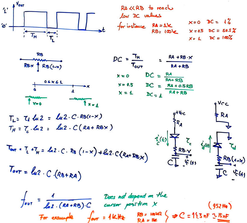
Fig. 7. Oscillator based on the classic IC 555 that allows the duty cycle modulation of the output waveform. We can determine TH and TL to observe how the duty cycle is modulated using the parameter x associated to the potentiometer cursor position. In this simple analysis we suppose ideal small signal diodes as perfect switches. |
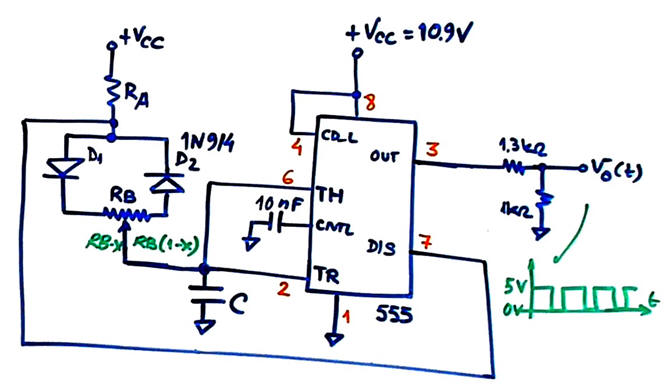
We can power the circuit using VCC = 10.9 V and we can adjust the VCNTL = 5 V (or 3.3 V changing the amplifier transconductance G = 0.3 S) to imagine the digital voltage that in next design phases will be supplied by the microcontroller. Try this PWM_555.pdsprj where the potentiometer modulates the duty cycle from 1% to 99%.
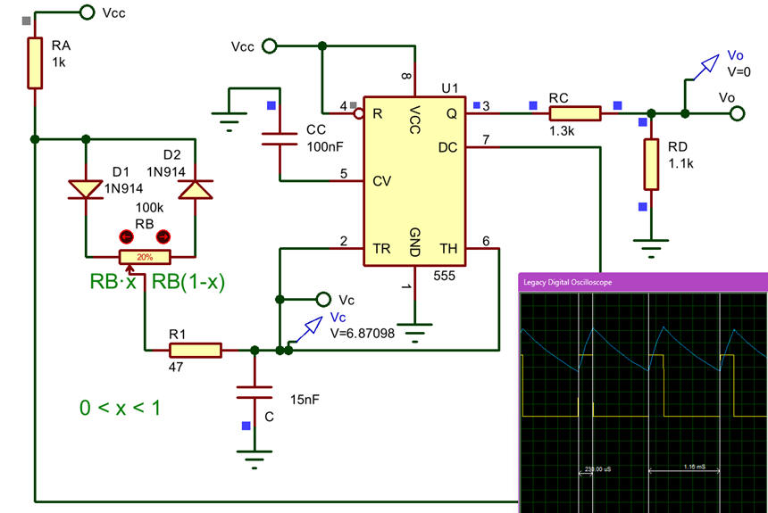
Fig. 8 shows the circuit capture. This is a good time to check the validity of the selected values and calculated expressions using the frequency meter, oscilloscope and other instruments.
|
|
|
Fig. 8. Prototype of the PWM circuit. |
The next step is to build the PWM prototype and verify its operations before using it to drive the digital voltage for the dimmer power amplifier.
|
|
|
Fig. 9. Prototype of the power adapter to verify that it generates the modulated waveforms adjusting RB. |

And finally the complete circuit, with the PWM driving the dimmer power amplifier.
|
|
|
Fig. 10. Analogue dimmer circuit ready for a table lamp. The 555 modulator is driving the power LED amplifier. The light intensity varies accordingly to the potentiometer RB. |

The next stage will aim to replace the analogue 555 chip by digital circuits to make it simpler to adjust the light intensity using push-buttons or rotary encoders.
|
|
Design phase B: Digital lamp ON/OFF and PWM control |
1. B specifications |
The new goal now is to replace the analogue PWM generator propose above in A1.2, by a digital circuit that will drive the power amplifier A1.1 under the same conditions. We can use microcontrollers or FPGA.
To visualise alternative designs and be able to compare features, we can imagine up to five options:
Option #B1: PWM control with FPGA and VHDL. Let us use the DE10_Lite FPGA board to provide a digital control of the lamp. The idea is to adapt the PWM architecture used by the PIC18F peripheral. This project is proposed and solved as version B at CSD D2.5.
|
|
|
Fig. 11. Prototype of the digital PWM control synthesised in FPGA. |

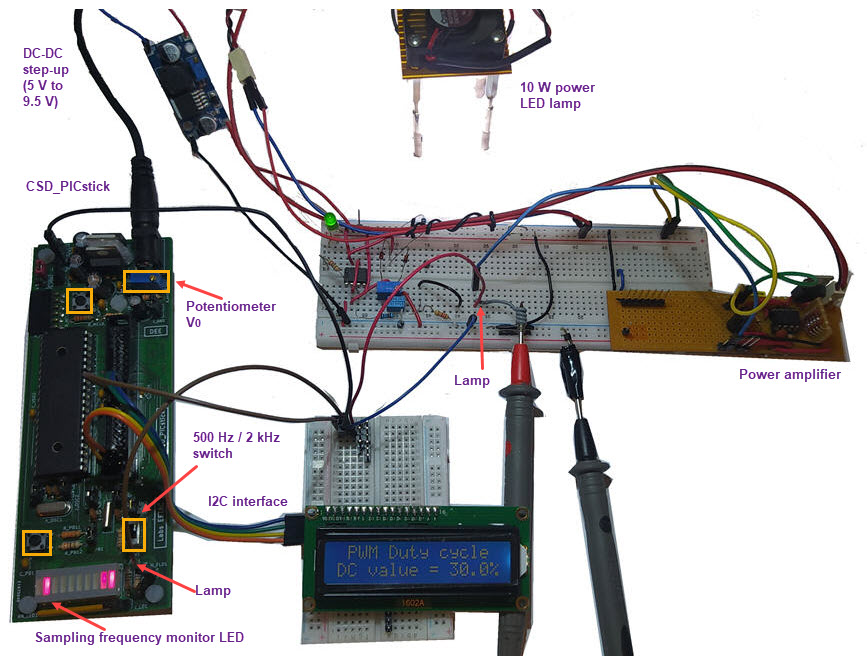
Option #B2: PWM control with PIC microcontroller. Let us use a CSD_PICstick board to provide the digital control of the lamp, as if this project were the CSD D3.5 continuation.
|
|
|
Fig. 12. Prototype of the digital PWM control running on the CSD_PICstick. |
Option #B3: Arduino. Let us use an Arduino board to provide the digital control of the lamp as it is usual for many hobbyist applications.
We can imagine similar design steps as in Option #B2.
Option #B4: Raspberry Pi.
Option #B5: SoPC NIOS-II. Let us come back to the FPGA design in Option #B1, embedding the microcontroller system in the FPGA.
|
|
Design phase C: Power supply adapter |
1. C specifications |
The previous design phases could have been experimented using a laboratory power supply. In this phase we aim to design the switching mode power supply for the power LED lamp.
The simplest way to obtain the required VCC = 10.9 V @ 1 A to power the lamp keeping high efficiency is to use a standard mains to USB adapter (5 V - 2 A), for example from an old phone or similar product and add a step-up converter to adjust the required voltage to VCC.
|
|
|
Fig. 12. Adjusting 10.9 V - 1 A from a 10 W USB wall adapter. A 10 Ω power resistor can be used as a load to experiment and verify connections. |
Another way is to design an specific power adapter for the lamp. We can step-down adjusting the required VCC = 10.9 V from an old PC 18 V - 35 W power supply adaptor.
|
|
|
Fig. 12. 20 W adjustable DC-DC step-down switch-mode Buck converter. (ref.). With this power available we can try to dim two LED lamps working in parallel or in series. |

|
|
Design phase D: Communication interfaces |
1. D specifications |
Our goal is to command the Dimmer using a wireless interface and a computer or an Android app. How to send Up and Down commands to the Dimmer?
| Home Contact Tutorials Electronic devices and companies Books Magazines Instruments Digsys Library EETAC DEEL |

|
|
| Web activa des de 01/2023, @ F. J. Robert. Web editat amb Microsoft Expression Web 4. El contingut és material de referència per al disseny d'equips electrònics. Llicència:Reconeixement 4.0 Internacional de Creative Commons |