|
|
Bachelor's Degree in Telecommunications Systems and in Network Engineering |
|
|
|
|||||
Chapter 2 problems |
- D2.23 - |
Earbuds control buttons (FPGA-VHDL) |
|||
|
|
|||||
1. Specifications
Design the button decoder (Button_controller) that is typical in many commercial Bluetooth earbuds. The idea is to assign a binary code to each function once detected. Fig. 1 shows a typical pair of commercial earbuds.
The same project designed programming a μC is in D3.23.
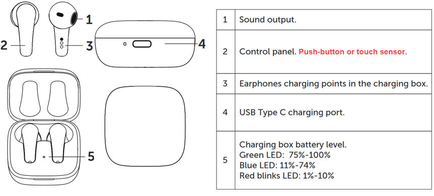 |
| Fig. 1. Example wireless commercial earbuds. Only one tactile pushbutton or capacitive touch sensor is available for commanding operations. |
Once paired, depending on the apps selected in the mobile phone, earbuds can be used for answering phone calls, voice assistance or playing music.
Let us simplify the option #1 in Fig. 2 where only typical music player functions are listed.
Option #1 example functions and actions:
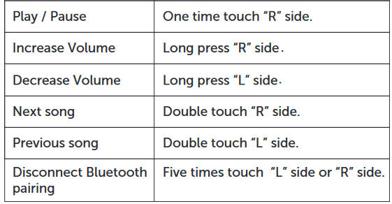 a) |
| Fig. 2 a) Example especifications when used as music player. |
Option #2 example functions and actions for multiple applications: call, music, gaming.
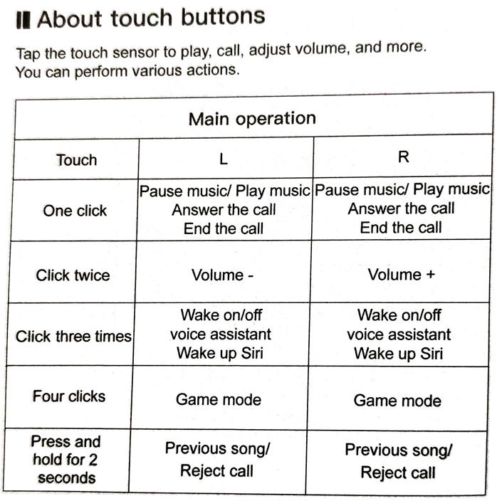 b) |
| Fig. 2b) Example functions when used for phone, music and gaming apps. |
An internal switch S may be used to select left or right earbuds. For example S = '0' is the right earbud, S = '1' is the left earbud.
The idea is organise a FSM to detect one, two or five continuous short clicks, and also a long press. Fig. 3 shows a block diagram of an earbud from Toshiba company.
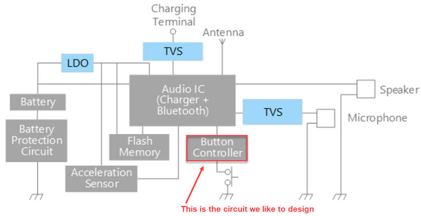 |
Fig. 3. Block diagram of an earbud. Reference paper: wireless earphone solution for long time operation with a small battery on a wireless earphone. TVS stands for transient voltage suppressor diodes to prevent the destruction of the electronics due to electrostatic discharges (ESD). LDO is a low dropout voltage regulator. |
Experiment in a protoboard and characterise the signals from a typical push-button. What is the typical time duration of a short and a long pulse?
Probably a tactile button will generate digital noise that we can eliminate using a debouncing filter. Better tu run the FSM using clean short and long pulses.
2. Planning
A commercial product has to be organised planning several design phases.
Design phase #1: basic features.
Solve the circuit for the design step #1. Only when it is fully tested working correctly and reported, solve the design step #2.
Design step #1. Let us start detecting (1) a single short click, (2) two short clicks and (3) a single long click.
Design step #2. (Optional) Add the five short clicks detection to disconect the Bluetoth pairing and other features.
Let us solve design step #1. How the captured signal will look like? How many samples do you need to identify the three patterns. What is the typical short click duration? Draw some waveforms in a timing diagram as in Fig. 4.
Let imagine that a short click event duration is between 130 ms and 240 ms. Thus, a good sampling frequency is 8 Hz ( TCLK = 125 ms). In this way detecting a short click will generate one or two consecutive '1'. The same with the time separation between two clicks, let it be one or two consecutive '0'. We can also imagine that more that three consecutive '1' is a long click. In this way we can figure out the buffer size of the capture window.
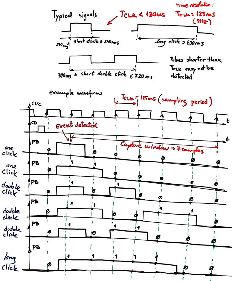 |
Fig. 4. Example timing diagram when clicking B several times. We can consider several situations, one short chick is one of two '1' detected. The separation between short clicks is one or two CLK periods. Thus, a signal capture window of seven samples is required before analysing the waveform and deciding which function assign. |
Once the event is detected, we need to assign the output function, depending on the earbud side (R / L). When one short click is detected in the right side (S = '0'), we need to toggle an internal play flag signal (P_Flag) to set the correct function code: Play or Pause. We can draw the Button_controller symbol and the function encoding as in Fig. 5. Function codes and function available pulse will be interfaced as inputs to the main earbud audio integrated circuit.
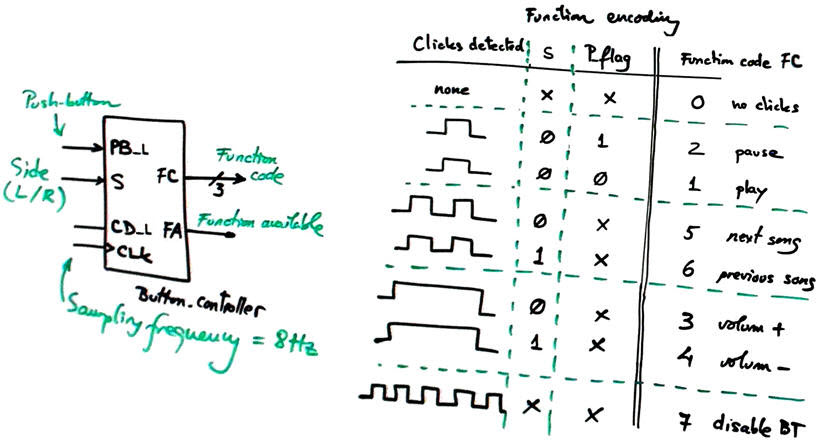 |
Fig. 5. Button_controller symbol and output function codes. |
With these initial ideas, we can try to fix an internal architecture as shown in Fig. 6. The first sampled '1' will allow to fill in click capture window. And after seven CLK cycles, the output function will be set. If the function detected is play or pause, the internal play flag will be updated.
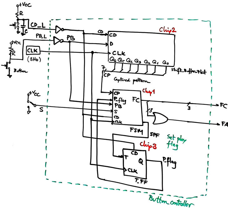 |
Fig. 6. Button_controller internal architecture. |
FSM
With such hardware resources we can imagine how the circuit will be commanded by the FSM.
Try to draw a state diagram for the circuit's FSM as shown in Fig. 7.
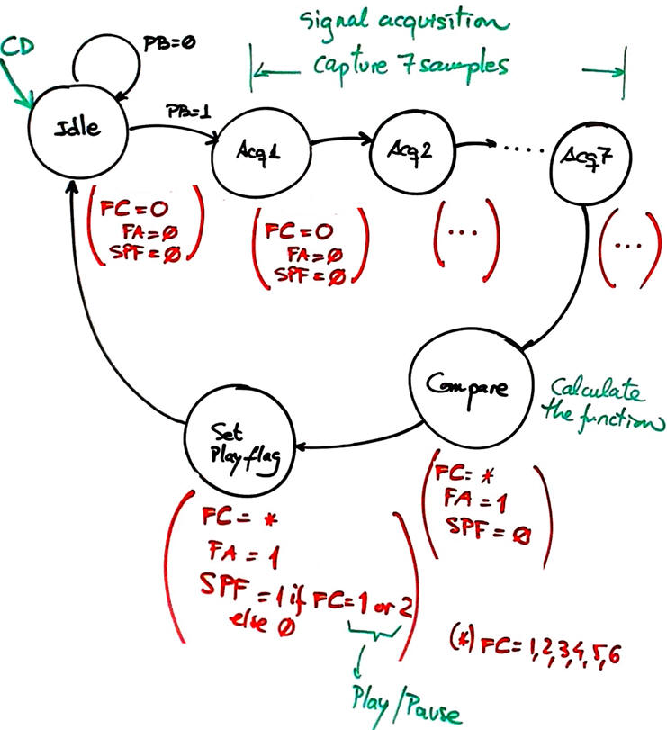 |
| Fig. 7. FSM example state diagram. |
Draw some waveforms in a timing diagram for the FSM.
 |
Fig. 8. Timing diagram showing several patterns captured. Some other captured patterns are represented in Fig. 4. The FSM will decide the function code assigned comparing the current pattern detected with models stored internally (CC2 truth table). |
Apply the FSM architecture to this problem.
Deduce how many D_FF are required when encoding FSM states using the following options and draw the state register memory:
Option #1: radix-2 (sequential)
Option #2: Gray
Option #3: Johnson
Option #4: one-hot
Draw the state register based on D_FF considering your state encoding option.
Write the truth table of CC2 and CC1 and their equivalent behavioural interpretations (plan B) using flowcharts. CC2 truth table will include the 7-bit comparator to set funcions codes. For instance, when the capture pattern is CP = "1111100" and S = '1', FC = "100" (volume -); when CP = "1000000" or "1100000" and S = '0' and P_flag = '1', FC = "010" (pause); etc.
Project location:
C:\CSD\P6\earbuds\(files)
Write the FSM VHDL file.
Start a Quartus Prime synthesis project for one of the following programmable target chips:
Option #1: Cyclone IV EP4CE115F29C7
Option #2: MAX II EPM2210F324C3
Inspect and annotate the RTL and technology views. Check the number of D_FF synthesised in this application.
Button_controller
Design or adapt the other components in the top entity Button_controller and synthesise and test it. For example, Fig. 9 shows how the left Shift_buffer_7bit.
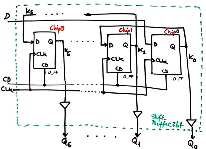 |
|
Fig. 9. Inventing the capture Shift_buffer_7bit chaining D_FF. |
Prepare a VHDL testbench fixture to adapt the stimulus signals in the Fig. 4 sketch. Rely on the constant CLK_Period for setting the time scale.
 |
|
Fig. 10. Testbench fixture. What inputs, outputs and internal signals are to be monitored? |
Run functional simulations to verify your design. Visualise as well in the wave timing diagram the internal states.
Measure the propagation time CLK to output (tCO)using gate-level simulations.
What may be a good estimation of the maximum frequency of operation? Explain your answer.
And more questions... for example, what will happen if the user clicks continuously the push-button? What can be done to prevent such situation?
Design phase #2: Additional features to enhance the product such crystal oscillator for CLK signals and timers for saving energy when the product is not used.
- Design step #1: Design a CLK generator to obtain the 8 Hz square wave from a 50 MHz quartz crystal oscillator like the one available in the DE10-Lite board. Deduce the number of D_FF that the Sequencer will contain.
- Design step #2: Replace the Shift_buffer_7bit by a shift register.
- Design step #3: Add a timer so that after 2 minutes in pause mode, the system goes a new sleep state to save battery energy.
| Home Term 24/25-Q1 Contact Products Electronic devices and companies Software Books Magazines Instruments DEE Library EETAC DEEL |

|
|
| Web activa des de 09/2001, @ F. J. Robert, J. Jordana. Web editat amb Microsoft Expression Web 4. El contingut és un complement als materials d'estudi del curs Circuits i Sistemes Digitals disponibles al campus digital Atenea. Llicència:Reconeixement 4.0 Internacional de Creative Commons |