|
|
Bachelor's Degree in Telecommunications Systems and in Network Engineering |
|
|
|
|||||
Chapter 2 problems |
- A2.3 - |
Analysis of an asynchronous circuit (Circuit_D) |
|||
|
|
|||||
1. Specifications
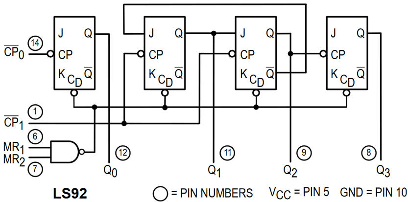
Fig. 1 represents the internal circuit of chip 74LS92 containing several chained flip-flops from its datasheet. Let us adapt it as usual to our naming style and conventions.
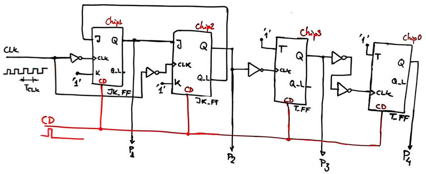
We can use our set of tools to analyse Circuit_D represented in Fig. 2 built using this chip resources and external logic gates.
 |
|
Fig. 1. 74LS92 chip equivalent internal circuit. |
Read its datasheet to determine how does it work (what is the funcion of each pin). Some J and K inputs are not driven, let us assume that they are connected to '1'.
Analyse Circuit_D in Fig. 2 using method II: Proteus capture and simulation, or method III: VHDL synthesis and test. Determine how does the circuit work, meaning finding the vector output P(4..1) in a clocked (CLK) timing diagram.
What is the maximum CLK frequency when picking the PLD target chip indicated below?
- Cyclone IV
- MAXII
Test your solutions using method I: handwritten analysis.
 |
|
Fig. 2. Circuit_D to be analysed using our three methods. |
| Home Term 24/25-Q1 Contact Products Electronic devices and companies Software Books Magazines Instruments DEE Library EETAC DEEL |

|
|
| Web activa des de 09/2001, @ F. J. Robert, J. Jordana. Web editat amb Microsoft Expression Web 4. El contingut és un complement als materials d'estudi del curs Circuits i Sistemes Digitals disponibles al campus digital Atenea. Llicència:Reconeixement 4.0 Internacional de Creative Commons |