|
|
Bachelor's Degree in Telecommunications Systems and in Network Engineering |
|
|
|
Soldering and prototyping |
Logic probe for experimentation
| Prototype specifications | Planning | Development, simulation and prototyping | Lab activities |
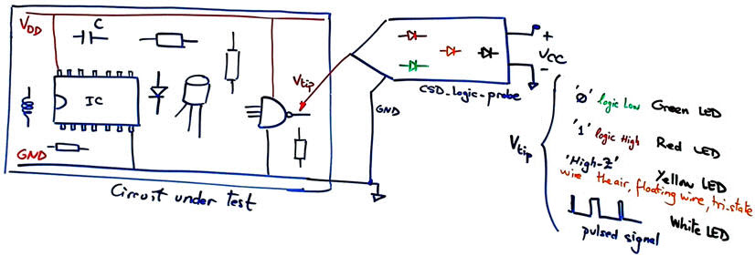
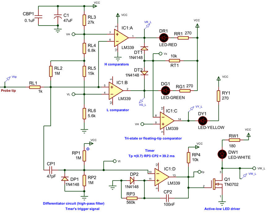
Laboratory prototyping is a fundamental phase in circuit design. To practise using lab tools and develop foundational skills, we will solder components onto a printed circuit board (PCB). For this project, we will design a simple instrument: a logic probe to visualise logic values and detect digital signals.
- High logic level: indicated by a red LED.
- Low logic level: indicated by a green LED.
- Tri-state, floating voltage or the probe tip in the air: indicated by a yellow LED.
- Oscillating digital signals: indicated by a white LED.
- Compatibility: fully CMOS and TTL compatible.
 |
|
Fig. 1. Logic probe symbol. |
| Specifications | Planning | Development, simulation and prototyping | Lab activities |
Planning steps are required for both designing the logic probe and developing the prototype. The same steps will be followed for soldering and verifying the probe prototype.
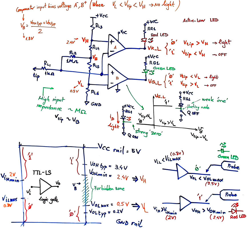
Using a versatile analogue comparator like the LM339 that can work from 2 V to 20 V allows compatibility with CMOS and TTL logic families.
Logic probe circuit
Step #1: detecting logic '1' and '0'
 |
|
Fig. 2. Basic comparator for measuring high and low digital voltages. |
Activity #1: Calculate the resistor network RL3, RL4, RL5, RL6 to adjust LS-TTL digital voltages. Calculate RG1 and RR1 limiting resistors to illuminate at nominal current standard 5 mm LED.
The bill of materials for this step #1 is in this file: "BoM_step1.txt".
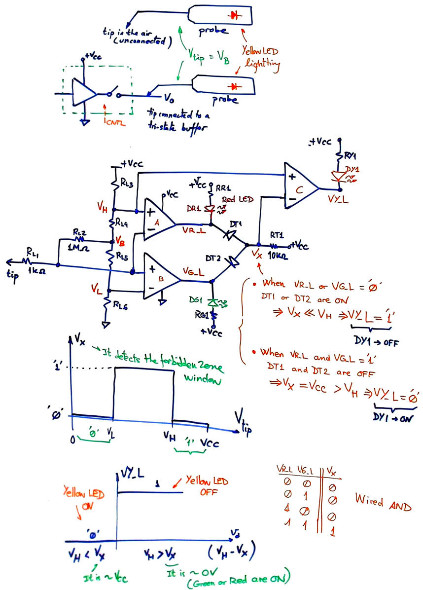
Step #2: detecting tri-state outputs or the probe tip in the air
Tri-state logic gates are discussed in lecture L5.4. The idea is to switch off both MOS transistors, leaving the output wire in the air or unconnected at a high-impedance state. Our circuit will detect when the input voltage is in the forbidden zone, or with the probe tip in the air, not sensing a valid zero or one.
 |
|
Fig. 3. Forbidden zone detector with a yellow LED and a wired AND function. |
The bill of materials for this step #2 is in this file: "BoM_step2.txt".
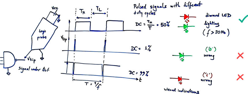
Step #3: detecting oscillating digital waveforms
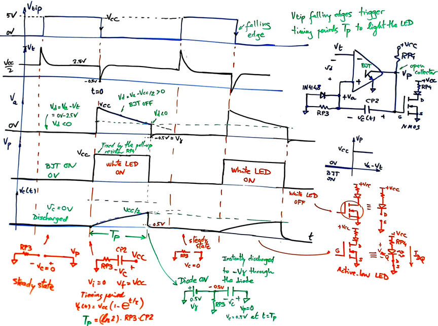
When the probe tip measures a digital waveform, both the green and red LEDs alternate. While this blinking is easy to visualize at low signal frequencies, higher frequencies cause the human eye to perceive the light pattern as continuous. Consequently, both LEDs will appear to light up simultaneously. Their relative brightness depends directly on the signal's duty cycle, as illustrated in Fig. 4. If the duty cycle is extremely small () or large (), only one LED will visibly light up, leading to the false interpretation that the signal is static.
 |
|
Fig. 4. Digital indications visualised by the logic probe for pulsed signals with different duty cycles. |
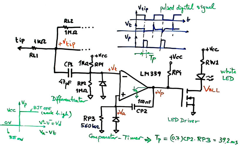
To resolve this limitation, an additional detector can be implemented, for instance, by utilizing the remaining comparator in the chip LM339N. The proposed circuit in Fig. 5 consists of an edge detector and a timer. The comparator output drives an active-low white LED via an NMOS transistor. This white LED remains constantly illuminated whenever an oscillating signal is detected, ensuring reliable pulse detection across a wide range of frequencies and duty cycles.
 |
|
Fig. 5. First-order high-pass filter as a differentiator to detect sharp signal edges and trigger timer pulses of TP duration. |
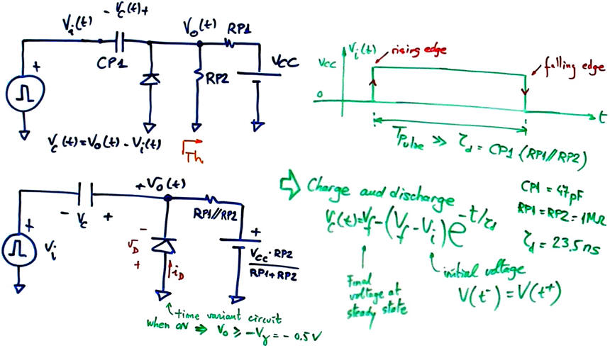
We can start studying the differentiator and how it can trigger the timer. The analysis of such circuit may be considered imagining that the network is driven by a VCC step signal. As shown in Fig. 6, the probe tip pulse the pulse is large enough to allow final steady states.
  |
|
Fig. 6. Analysis of the simplified idealised pulse detector circuit. |
The diode prevents excessive negative voltages; it keeps Vo above the threshold -0.5 V. This negative voltage is enough to trigger the timer on the pulse falling edge.
 |
|
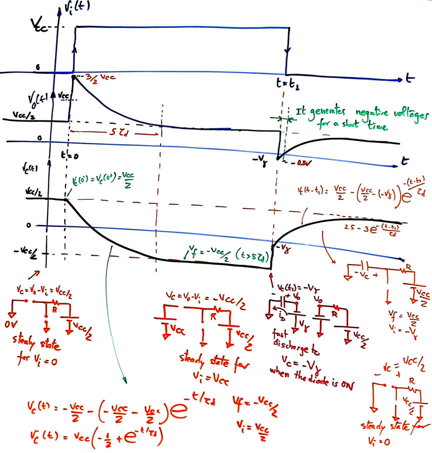
Fig. 7. Using the same capacitor's charge and discharge equation and steady state equivalent circuits, we can deduce the duration TP of the timing period. |
Now it is time to visualise all the waveforms and validate calculations using the Proteus simulator.
This is an example on how you can integrate concepts from ET (1A) and CSL (1B) with the purpose of inventing a simple and useful instrument for your new CSD (2A) course projects.
The bill of materials for this step #3 is in this file: "BoM_step3.txt".
Note: Operation up to 15 V or 18 V CMOS technology is possible by recalculating the LED current-limiting resistors to maintain nominal current. In the same way, the comparator resistor network can be adjusted to other logic families of interest.
Activity #2: Calculate the resistor network RL3, RL4, RL5, RL6 to adjust 18 V CMOS digital voltages. Calculate the LED limiting resistors to bias the four LEDs at a nominal current of 10 mA.
| Specifications | Planning | Development, simulation and prototyping | Lab activities |
First, we will simulate the circuit in Proteus to validate the design and adjust the components.
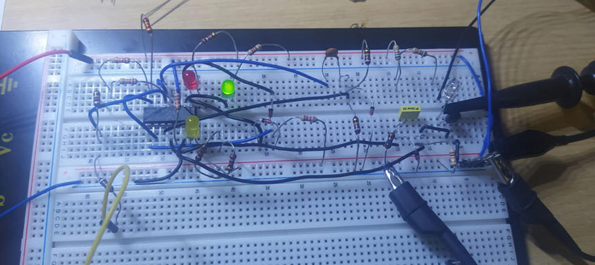
Second, we mount the prototyping board to verify that it works as expected.
Third, we design a PCB to solder all the components and practise basic lab skills.
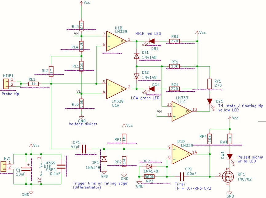
Circuit capture and simulation in Proteus
This is the "Logic_probe_prot_v1.pdsprj" copied in Fig. 8. It contains a tri-state chip to be connected to the probe tip probe to test the yellow LED. You can also try with zeros and ones. A signal generator allows stimulating the circuit with digital signals to validate the white LED detector. The circuit can be captured and tested following the three design steps.
Many measurements can be performed in simulations: LED currents, reference voltages, frequency response, supply voltage range, etc.
 |
|
Fig. 8. Complete circuit captured in Proteus. |
Protoboard experiment
Validating the circuit with a laboratory experiment. Generally, the real circuit behaves practically like the simulated one; most of the design errors and adjustments were detected and corrected in the previous simulation stage. However it is still worth to mount it in a protoboard.
 |
|
Fig. 9. The protoboard contains all the logic probe components. |
Printed circuit board (PCB)
And finally, the most interesting project phase: on the design of the PCB to solder all the materials and make it looks like a professional logic probe.
You can install KiCad, and learn to use it precisely copying and adapting files and components from this sample project. In the same way, you can install FreeCAD to add 3D models to each footprint.
This is the KiCad project "CSD_logic_probe_PCB.zip".
NOTE: Our current CSD and DEE KiCad symbols, footprints, and 3D components are available in the library "DEE_libraries.zip" which can be unzipped and saved using these KiCad installation instructions. Basically, at this introductory PCB design level, the idea behind tuning component footprints is to enlarge their pads to make soldering easier.
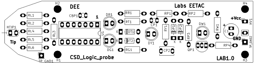
The PCB design starts capturing the schematic in KiCad as shown in Fig. 10.
 |
|
Fig. 10. Schematic captured in KiCad. |
The PCB component placement is shown in Fig. 11.
 |
|
Fig. 11. PCB layout silkscreen that shows component placement and their references. |
Finally, a 3D view shows how the PCB will look like once soldered.
 |
|
Fig. 12. PCB 3D representation. |
Additionally, we can set several parameters for easy routing, manufacturing and soldering, such clearance between components and tracks (0.3 mm), and signal (0.5 mm) and power (1 mm) track widths.
Fig. 13 shows the process of placing and soldering components on the board's prototype once manufactured using our lab machines. At this stage, we have to verify that the board works as expected or, if it is the case, make the necessary adjustments.
 |
| Fig. 13. PCB produced at EETAC labs and soldered to validate the circuit. |
These are all the board components in CSV format exported from KiCad including commercial references and datasheet information.
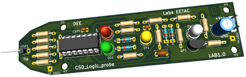
Once this final revision step is completed, the PCB is ready for manufacturing as shown in Fig. 14.
|
|
| Fig. 14. The final manufactured board with the silkscreen layer labels printed to easily identify where all the components are placed. |
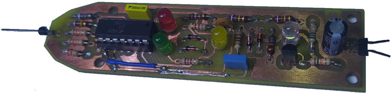
Board's picture in Fig. 15 shows the current prototype board with all the soldered components.
| Fig. 15. The idea of placing and soldering components on the PCB. The final manufactured board with the silkscreen layer labels printed. |
| Specifications | Planning | Development, simulation and prototyping | Lab activities |
Step #1 Soldering the components of the basic High-Low probe.
| Fig. 16. Manufactured PCB and kit of components for the step #1. |
| Fig. 17. Box of tools. |
| Fig. 18. Step #1 components soldered. |
Validation
Let us validate the detection of high and low digital values powering the probe and using the function generator.
| Fig. 19. Wiring the probe and testing low and high digital values. |
Step #2 Soldering the tri-sate components
Validation
Step #3 Soldering the pulsed signals detector
Validation
| Home Term 26/27-Q1 Contact Products Electronic devices and companies Software Books Magazines Instruments DEE Library EETAC DEEL |

|
|
| Web activa des de 09/2001, @ F. J. Robert, Web editat amb Microsoft Expression Web 4. El contingut és un complement als materials d'estudi del curs Circuits i Sistemes Digitals disponibles al campus digital Atenea. Llicència:Reconeixement 4.0 Internacional de Creative Commons |