|
|
Bachelor's Degree in Telecommunications Systems and in Network Engineering |
|
|
|
Design Circuit_P using plan A |
Circuit_P plan B |
Circuit_P plan C2 |
| 1. Specifications | Planning | Developing | Testing | Report | Prototype |
Using Circuit_P truth table written in Fig. 1 invent the following equivalent circuits using gates (plan A):
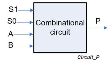 |
Fig. 1. Circuit_P symbol and truth table. |
 |
|
- Circuit_P1. Draw the equivalent circuit using product of maxterms. Check it using method III tools.
- Circuit_P2. Design an equivalent minimised circuit based on SoP. Check this circuit or its equation using method II tools.
| Specifications | 2. Planning | Developing | Testing | Report | Prototype |
Drawing the circuits that represent the canonical equations are inferred once the truth table is known.
1. Circuit_P1. Use the product of maxterms expression to draw the circuit composed of a regular network of BUFFER-NOT/OR/AND. All OR gates (maxterms) are of 4 inputs. A single AND gate is required. Regular and canonical circuit of three levels of gates.
C:\CSD\P1\Circuit_P\Circuit_P1\(files, pictures, etc.)
2. Circuit_P2. Use minilog to minimise P = f(S1, S0, A, B) as a SoP and draw the circuit. This is the project location:
C:\CSD\P1\Circuit_P\Circuit_P2\(files)
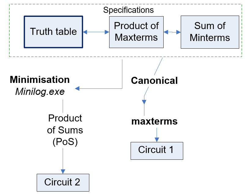 |
| Fig. 2. Planning the design process for Circuit_P1 and Circuit_P2. |
| Specifications | Planning | 3. Developing | Testing | Report | Prototype |
Circuit_P1. The product of maxterns is: P = M3 · M5 · M6 · M7 · M8 · M11 · M14 · M15
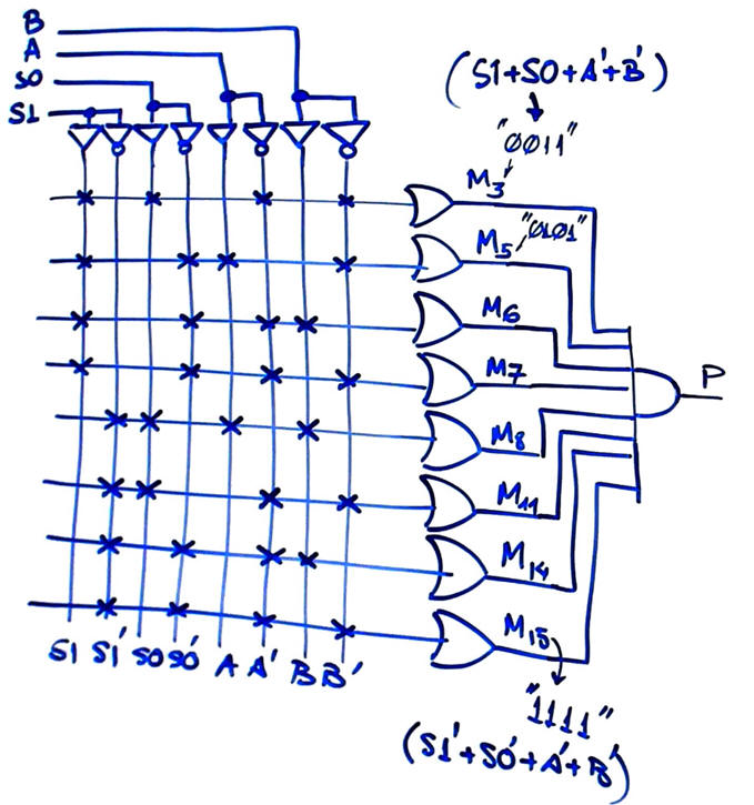 |
| Fig. 3. Circuit_P1 based on the product of maxterms. |
Circuit_P2. Circuit_P2.tbl is used as the input file for minilog to obtain the simplified SoP equations and its circuit representation:
 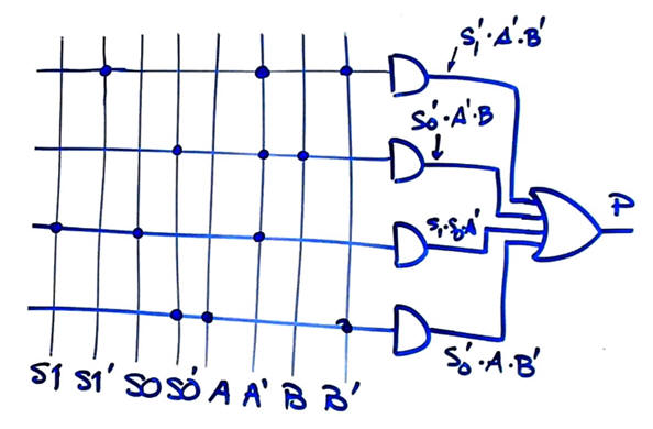 |
| Fig. 4. Circuit_P2 based on SoP |
| Specifications | Planning | Developing | 4. Testing | Report | Prototype |
1. Validating Circuit_P1 using VHDL.
The Circuit_P1.vhd equation using product of maxterms as a VHDL source file. Remember that this is the project location:
C:\CSD\P1\Circuit_P\Circuit_P1\(files)
After the synthesis process, you can see the RTL view, the schematic that looks like the equation described in the architecture.
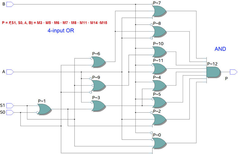 |
Fig. 5. Example of an RTL schematic on the product of maxterms. |
And also the tecnology view ajusted to a given FPGA chip. This 4-input funcition is modifyed by Quartus Prime synthesiser and implemented in a single logic cell (look-up table).
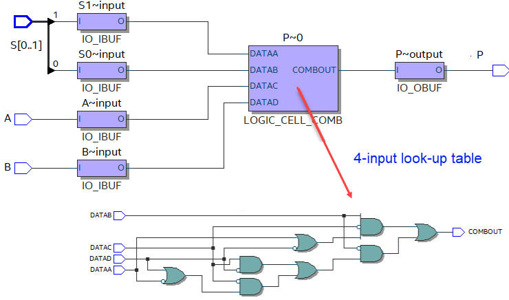 |
Fig. 6. Example of an RTL schematic on the product of maxterms. |
We can proceed testing the circuit using a VHDL testbench such Circuit_P1_tb.vhd.
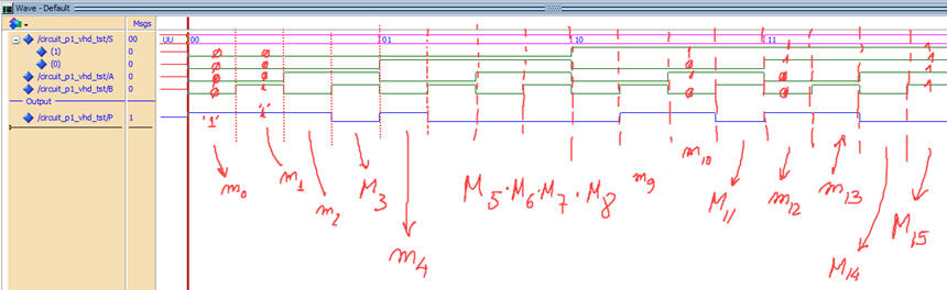 |
| Fig. 7. Waveforms from the timing diagram in ModelSim that verifies the correction of Circuit_P1. |
2. Validating Circuit_P2 using method II tools such Proteus Circuit_P2.pdsprj based on SoP. Run simulations to complete its truth table.
C:\CSD\P1\Circuit_P\Circuit_P2\(files)
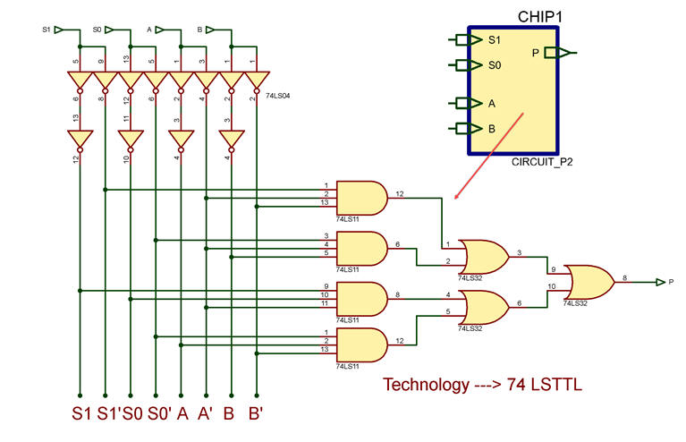 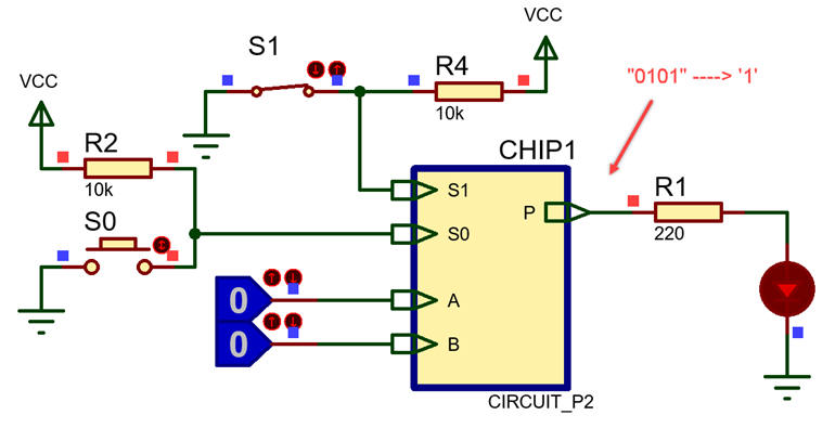 |
| Fig. 8. Capturing Circuit_P2 in Proteus and results for a given combination S1 = '0'; S0 = '1'; A = '0'; B = '0' |
| Specifications | Planning | Developing | Testing | 5. Report | Prototype |
Follow this rubric for writing reports.
| Specifications | Planning | Developing | Testing | Report | 6. Prototype |
We can use the DE10-Lite board to implement this project, as shown in Lab 1.2 for the similar Circuit_W.
| Home Term 26/27-Q1 Contact Products Electronic devices and companies Software Books Magazines Instruments DEE Library EETAC DEEL |

|
|
| Web activa des de 09/2001, @ F. J. Robert, Web editat amb Microsoft Expression Web 4. El contingut és un complement als materials d'estudi del curs Circuits i Sistemes Digitals disponibles al campus digital Atenea. Llicència:Reconeixement 4.0 Internacional de Creative Commons |