|
|
Bachelor's Degree in Telecommunications Systems and in Network Engineering. Bachelor's Degree in Aerospace Systems Engineering |
|
|
Power lamp PWM control using FPGA and VHDL tools |
| 1. Specifications | Planning | Developing | Test functional | Test gate-level | Report | Prototype |
This is the full project page for the Dimmer's Option #B1: hardware design. Let us use the DE10_Lite FPGA board to provide a digital control of the lamp, as if this project were the CSD D2.5 continuation.
-
10-bit maximum PWM resolution. 8-bit PWM resolution at 1 kHz.
-
10-bit frequency adjustment using a switch array.
-
Electrical isolation to the power driver using an optocouple.
-
UP-DOWM push-buttons for PWM adjustment. Sweep all PWM values in 5 s.
|
|
|
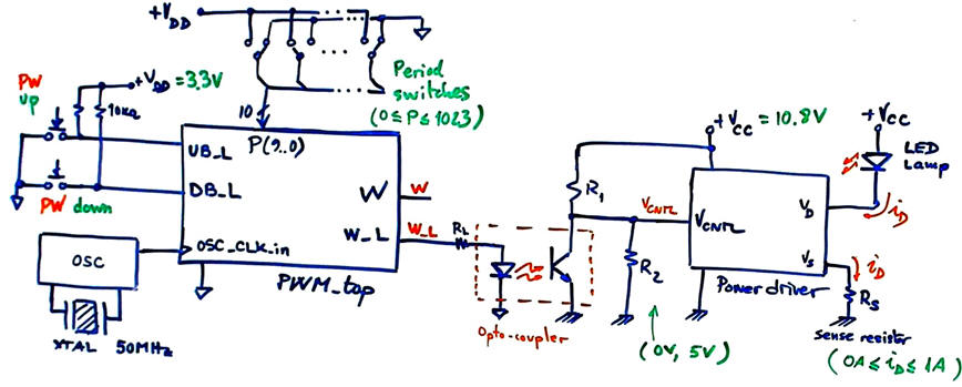
Fig. 1. PWM_top circuit for controlling the light intensity of the LED lamp. The PWM waveform is connected to the power driver using a phototransistor coupler adapting control voltage levels at the same time. |
| Specifications | 2. Planning | Developing | Test functional | Test gate-level | Prototype | Report |
The top circuit will provide a mechanism for adjusting the DC and the waveform frequency fW. For instance, two push-buttons UP and DOWN to sweep all the values
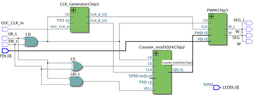
To make it simpler, we can design the top structure PWM_top using several blocks as usual in plan C2. The basic element will be the PWM module controlled by 10-bit vector inputs PW and P for fixing the pulse width and the signal frequency. A reversible 10-bit counter activated by two push-buttons will set the pulse width. The CLK_Generator will be in charge of synthesising the required frequencies for the PWM time-base and the push-button counter circuit.
|
|
|
Fig. 2. PWM_top internal architecture using three subcircuits and combinational logic. Using a CLK_PB frequency of 200 Hz, we can seep all PWM values in 5 s. |

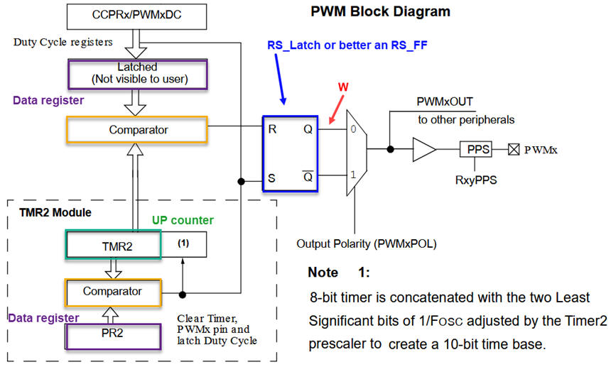
The PWM module will be conceived as an adaptation of the PWM-TMR2 Microchip PIC18F diagram copied in Fig. 3. from this technical brief reference: Barbulescu, G., Bujor, I., "TB3270: Getting Started with PWM Using CCP on PIC18", Microchip.
|
|
|
Fig. 3. PWM symbol and diagram of the PWM peripheral for PIC18F microcontrollers. The period value P and the pulse width value PW are 10-bit vectors. They will adjust respectively the waveform frequency fW and its duty cycle DC. |

And thus, Fig. 4 shows the adaptation using standard component products from CSD. This schematic is ready for VHDL translation and development along with the other modules in the PWM_top.
|
|
|
Fig. 4. Internal architecture proposed for the PWM module. Is is adapted from the TMR2-PWM idea. |
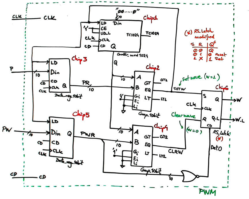
In this circuit there is no need of a FSM to control the device. It works nonstop. P and PW values are sampled and registered when resetting the waveform to start a new period (SETW signal).
As shown in Fig. 5, from these circuits we can deduce the output waveform W equations. And, from the specifications, we can deduce which are the convenient CLK frequencies to use.
|
|
|
Fig. 5. Example timing diagram and DC calculation. |

The CLK_Generator standard structure adapted from L8.2 is used to synthesise the CLK_PWM (257.8 kHz) and the CLK_PB (200 Hz).
Project location accordingly to the option:
C:\DEE\Dimmer\PhB_OP1\(files)
| Specifications | Planning | 3. Developing | Test functional | Test gate-level | Prototype | Report |
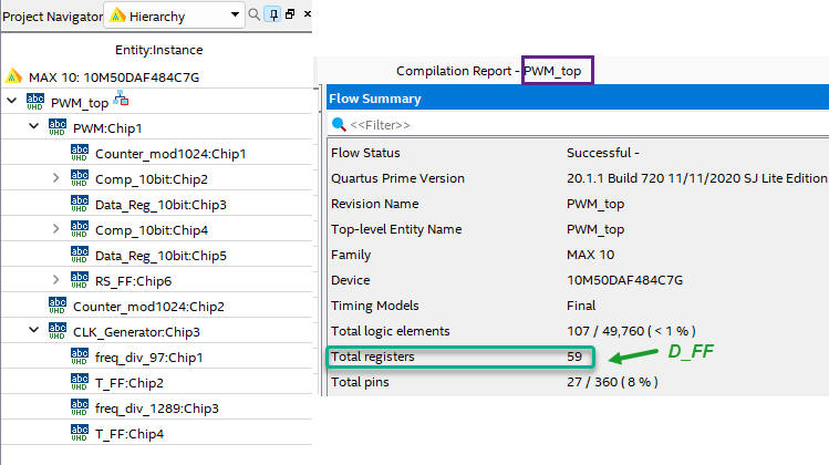
Let us translate the architectures above into VHDL, create a new hardware project for the MAX10 FPGA available in the DE10-Lite board, synthesise the circuit for the MAX10 PFGA. This is the full project "PWM_top.zip" including the pin assignment and a testbench.
|
|
Fig. 6. Resources used and the RTL view of the synthesised project output waveforms. Fig 7 shows an example of DC = 74% |
| Specifications | Planning | Developing | 4. Test functional | Test gate-level | Prototype | Report |
|
|
Fig. 7. Functional simulation using a testbench to drive the crystal oscillator and the push-buttons clicks. |

| Specifications | Planning | Developing | Test functional | 5. Test gate-level | Prototype | Report |
| Specifications | Planning | Developing | Test functional | Test gate-level | 7. Prototype | Report |
Assigning pins for the DE10Lite "PWM_top_prj.csv", we can program the FPGA with the "PWM_top.sof" or "PWM_top.pof" to run the prototype. We can take a picture of the full circuit running, as represented in Fig. 8.
|
|
Fig. 8. Circuit running experimenting the PWM modulation of the light intensity. The minimum frequency of 256 Hz is high enough for not observing light flicker. |
| Specifications | Planning | Developing | Test functional | Test gate-level | Prototype | 6. Report |
| Home Contact Tutorials Electronic devices and companies Books Magazines Instruments Digsys Library EETAC DEEL |

|
|
| Web activa des de 01/2023, @ F. J. Robert. Web editat amb Microsoft Expression Web 4. El contingut és material de referència per al disseny d'equips electrònics. Llicència:Reconeixement 4.0 Internacional de Creative Commons |