|
|
Bachelor's Degree in Telecommunications Systems and in Network Engineering |
|
P3: Arithmetic circuits in radix-2: adder, multiplier, comparator, etc. VHDL design plan C2: hierarchical structural modular multiple-file |
| Resources in lectures and labs: | L3.1, Lab3, L3.2, L3.3 | Project | objectives |
Highlighted project: 8-bit ones counter using plan C2
| 1. Specifications | Planning | Developing | Functional test | Gate-level test | Report | Prototype |
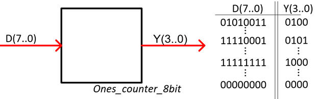
Design a circuit to count the number of ones in its 8-bit input vector using a hierarchical approach.
|
Fig. 1. Symbol and examples from the truth table of the 8-bit ones counter. |
This application can be used for example to count de number of free slots in a parking. Only the number of parked cars is important, not their current position in the parking.
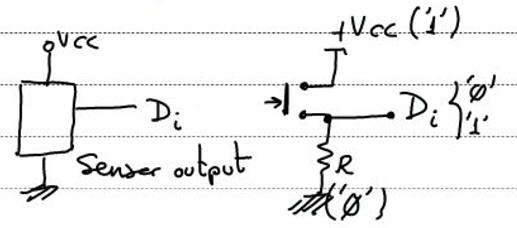
Inputs may be connected to contact switches, ultrasonic, radio or IR light sensors. Thus, they may be modelled imagining pushbuttons or switches as shown on Fig. 2. Outputs are represented in binary radix-2, however, it is easy to add a code converter from radix-2 to BCD to represent the number of counted ones in 7-seg displays.
|
|
|
Fig. 2. Pushbutton generating '0' and '1' to model digital sensors. |
Propose a circuit that at the same time can be expanded to a larger number of inputs, for instance 32 or 64 bit.
Other design tutorials and assignments.
| Specifications | 2. Planning | Developing | Functional test | Gate-level test | Report | Prototype |
Organise a hierarchical architecture for this circuit using smaller components. How many VHDL files will be required?
|
|
|
Fig. 3. Planning the application using components and signals. |
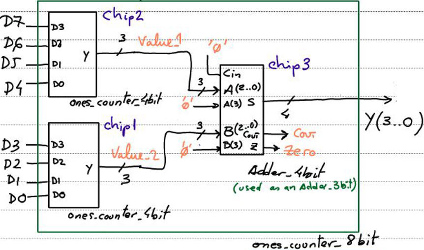
Therefore, this design requires three bottom-up steps:
1.- Design the project of the 4-bit ones counter using any convenient plan (A, B or C2). For example this is the design using plan C2 and the MoD: Ones_counter_4bits.
2.- Design the project of the 4-bit adder. Here you have two versions of this circuit base on plan C2: Adder_4bit ripple carry (RC), Adder_4bit carry lookahead (CLA).
3.- Translate the plan proposed in Fig. 3 into VHDL to be the top schematic.
Project location:
C:\CSD\P3\Ones_counter_8bit\(files)
| Specifications | Planning | 3. Developing | Functional test | Gate-level test | Report | Prototype |
This is the Fig. 3 translation to VHDL ones_counter_8bit.vhd.
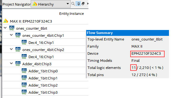
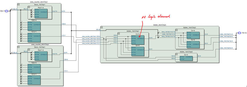
Run a EDA project to synthesise the circuit for a target chip, for instance MAXII EPM2210F324C3.
|
|
|
Fig. 4. RTL view once synthesised using Quartus Prime. |
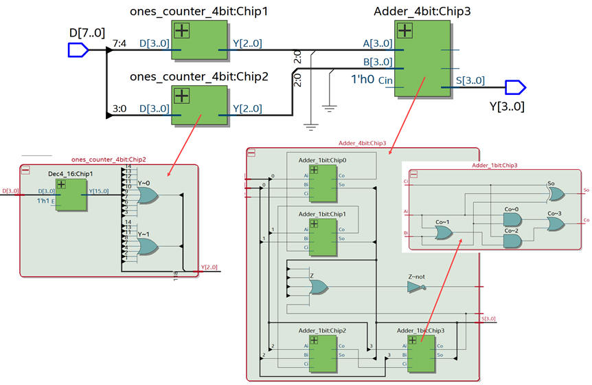
This design uses 11 logic elements.
|
|
| Fig. 5. Hierarchical component structure, technology view and resources used. |
| Specifications | Planning | Developing | 4. Functional test | Gate-level test | Report | Prototype |
The test bench fixture is used for organising the VHDL simulation project in ModelSim.
|
|
| Fig. 6. Testbench fixture. |
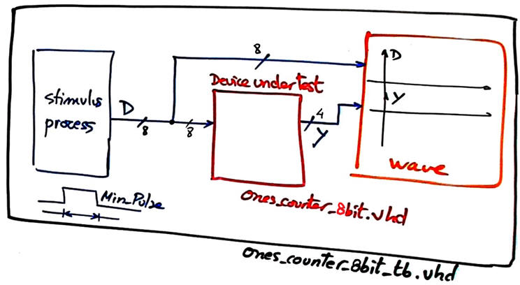
Translate the sketch of an example timing diagram to a VHDL test bench. This is an example from which to copy constant Min_Pulse and the input stimulus ones_counter_8bit_tb.vhd.
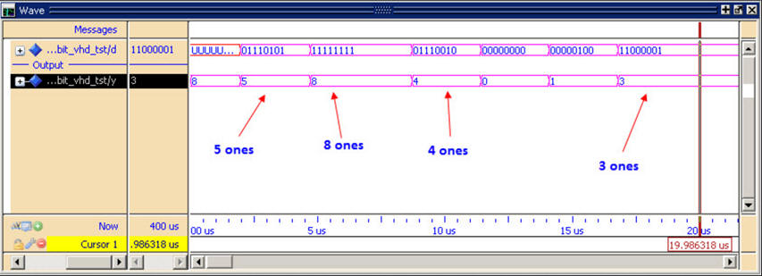
Discuss results on waves from the logic analyser tool.
|
|
| Fig. 7. Funcional results. |
| Specifications | Planning | Developing | Functional test | 5. Gate-level test | Report | Prototype |
Each PLD(FPGA has its electrical characteristics, thus the final performance will be related to the particular target chip specifications.
Propagation time measurements in a given transition
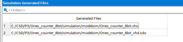
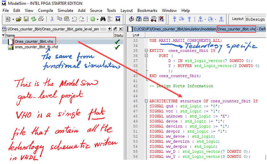
Let the synthesiser generate the EDA netlist file ones_counter_8bit.vho. And also the delay file: ones_counter_8bit.sdo.
|
|
| Fig. 8. Translation to VHDL of the technology view. |
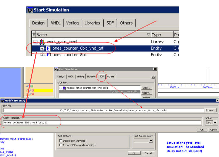
Let us start a gate-level (timing) simulation project with the library work_gate_level. Delay file must be assigned to the testbench entity.
|
|
| Fig. 9. SDO delay file assigned to the region. |
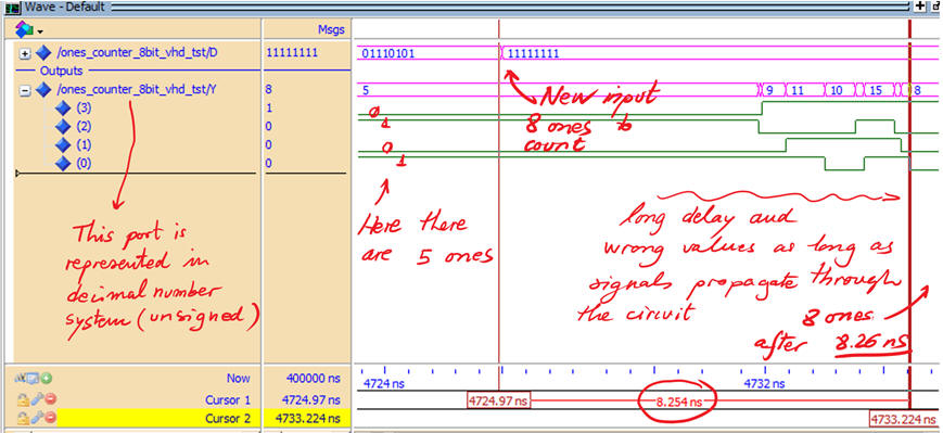
Run the logic analyser to observe the circuit behaviour at a given transition. As you see in Fig. 10, it takes the circuit 8.26 ns to obtain the correct count of ones when switching from input "01110101" to "11111111". And in between, there are several wrong output values while the signals are propagating through the chip structure.
 |
|
Fig. 10. Example of gate-level simulation where we can inspect the delay of the outputs at a given inputs transition. |
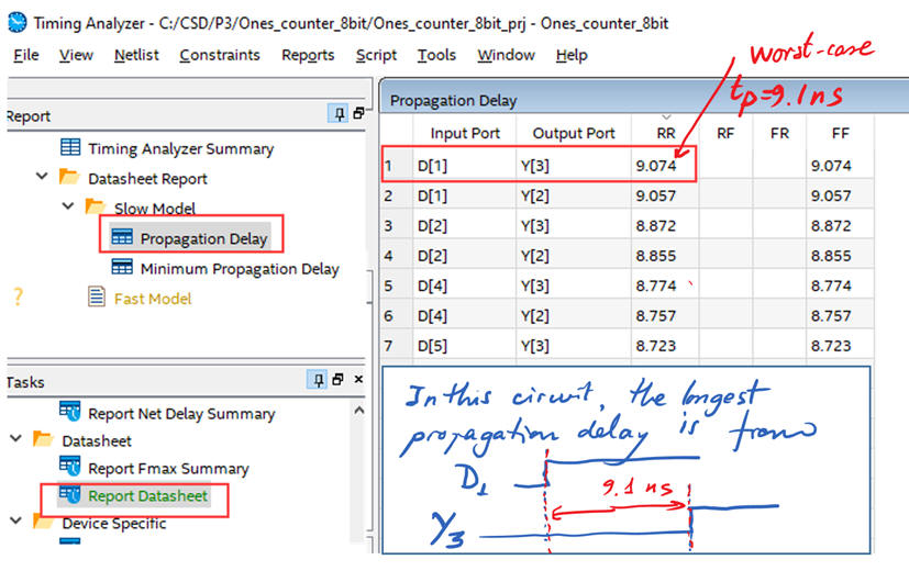
Timing analyser tool: longest propagation time and maximum speed of operation
EDA tool timing analyser available in Quartus Prime allows the measurement of the worst-case scenario propagation time (tP) and thus calculate the maximum speed of operation for the target technology.
In this example the maximum processing speed is 109 MHz (more than 100 millions of operations -counting the number of ones in the input vector- per second).
 |
|
Fig. 11 Timing analyser results. |
| Specifications | Planning | Developing | Functional test | Gate-level test | 6. Report | Prototype |
Follow this rubric for writing reports.
| Specifications | Planning | Developing | Functional test | Gate-level test | Report | 7. Prototype |
Use training boards and perform laboratory measurements to verify how the circuit works. Each specific board requires some kind of adaptation, for instance active voltage levels, multiplexed display systems, etc.
This DE10-Lite page explains how to install drivers and run an application.
Assign pins with the pin planner spreadsheet.
Generate the output SOF file and run the programmer. Lab 2 prototype shows you how to proceed with similar examples.
| Home Term 24/25-Q1 Contact Products Electronic devices and companies Software Books Magazines Instruments DEE Library EETAC DEEL |

|
|
| Web activa des de 09/2001, @ F. J. Robert, J. Jordana. Web editat amb Microsoft Expression Web 4. El contingut és un complement als materials d'estudi del curs Circuits i Sistemes Digitals disponibles al campus digital Atenea. Llicència:Reconeixement 4.0 Internacional de Creative Commons |