|
|
Bachelor's Degree in Telecommunications Systems and in Network Engineering |
|
|
Laboratory |
Laboratory 2: designing a standard MUX_8. Flat single-file VHDL: Plan A - Plan B - Prototype This is the reference highlighted project Hex_7seg_decoder [P2] solved using plan A |
[3/10] |
|
This is the post lab assignment PLA2 to be submitted next Lab 3. Study in detail and execute in your computer this lab tutorial and the reference design before attempting to solve the PLA. |
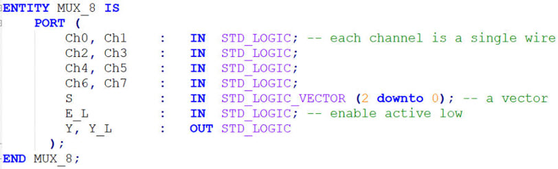
1.7.2. Multiplexer or data selector
| 1. Specifications | Planning | Developing | Testing | Report | Prototype |
Design a MUX_8 with characteristics similar to the classic 74HCT151 chip in a programmable logic device (PLD) target chip following structural plan A using our VHDL design flow and EDA tools for developing and testing.
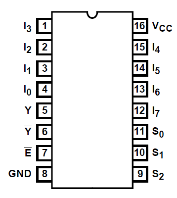 |
Fig. 1. Package and pin enumeration of classic 74HCT151 chip. We have to interpret and rename the pins because each company has its own way to name inputs/outputs and organise product datasheets (Nexperia, Toshiba/Renesas, ON semiconductor, Texas Instruments 74HCT151, etc.); thus, in CSD we have decided to use our own naming style and rewrite the truth table accordingly. For instance, the pin 12 will be always our input Ch7, an so the same with all the other pins. The technology of the logic family (TTL, LS, S, CMOS, AS, HC, HCT, F, etc.) is not important because the circuit will be targeted for a PLD from Intel, Xilinx or Lattice Semiconductor. Thus, only the chip functionality is considered. |
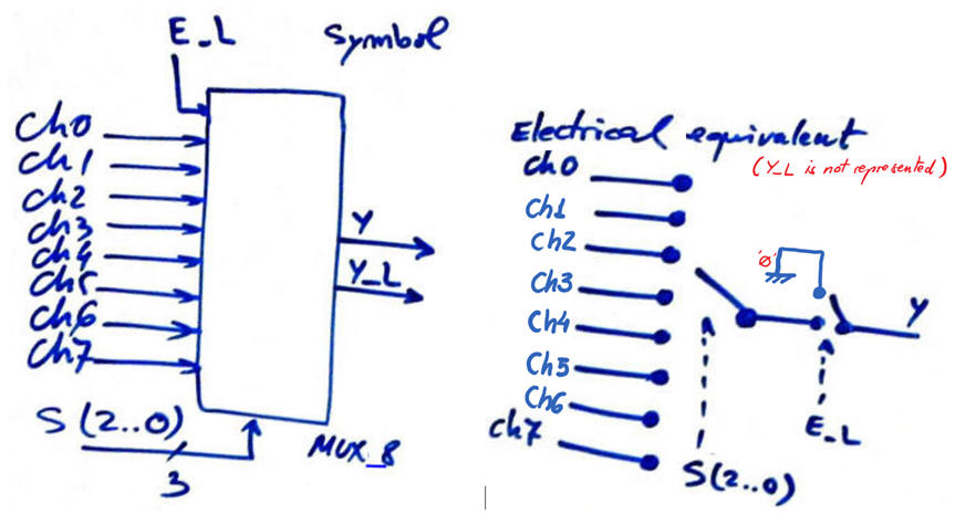
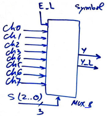
Fig. 2 shows our MUX_8 symbol.
|
|
| Fig. 2. Symbol adapted from datasheets. A multiplexer is a data selector. |
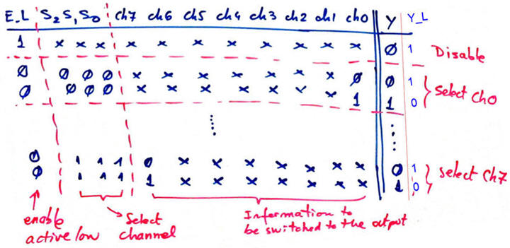
In Fig. 3 is represented the circuit's truth table using don't care terms.
|
|
|
Fig. 3. Truth table. The circuit has twelve inputs, it means 4096 binary combinations. |
|
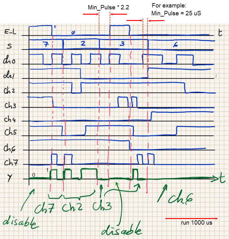
| Fig. 4. Example of a timing diagram sketch to demonstrate how the circuit works for different inputs. This input activity will be translated to VHDL as a stimulus process in the simulation testbench (Fig. 10). |
Find and study similar products, like MUX_16, MUX_4, MUX_2 and also demultiplexers.
In this project we will apply our VHDL design flow using plan A: flat (single-file) structural VHDL project. Take some time studying this specifications and how a structural plan will look like (rec.). Is it possible or easy) to write canonical equations based on minterms or maxterms?
This is the general concept map rec. to design most of CSD circuits.
| Specifications | 2. Planning | Developing | Testing | Report | Prototype |
Fig. 5. may be a sequence of operations for inventing MUX_8 in a single-file VHDL project using plan A.
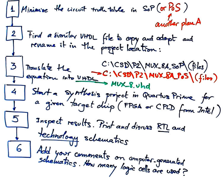 |
| Fig. 5. Planning the development (synthesis) of the circuit. |
The verification of the circuit under test may be carried out following Fig. 6 sequence.
 |
| Fig. 6. Testing procedure. |
- We have to find equations from circuit's truth table.
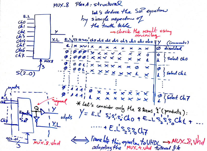 |
| Fig. 7. Schematic with equation SoP. Output Y_L is implemented using an inverter. Explain what is a port and what is a signal. |
Project location. For instance, you can save the project based on SoP here:
C:\CSD\P2\MUX_8A_SoP\(files)
Alternatively, other students may solve the project using PoS at the location:
C:\CSD\P2\MUX_8A_PoS\(files)
Find a similar VHDL circuit in P2 with an architecture that uses logic equations to copy and adapt.
| Specifications | Planning | 3. Developing | Testing | Report | Prototype |
Find minimised equations PoS or SoP running Minilog. This is an example Minilog file MUX_8.tbl capturing the truth table to obtain a simplified equation.
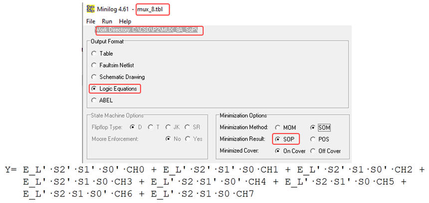 |
| Fig. 8. Minilog results in SoP format. |
Find a similar VHDL circuit file in P2 with an architecture that uses logic equations to copy and adapt. This is a VHDL translation source file MUX_8.vhd that corresponds exactly to our plan in Fig. 7 using SoP. The entity name is related to the symbol in Fig. 2. Note that in this symbol channel inputs are not considered as a vector but as individual wires.
 |
| Fig. 9. Description of the entity is the same for all design plans. |
KEY NOTE in CSD: Do not write VHDL code without the corresponding printed schematic / e equation / diagram / flowchart / algorithm from the previous planning section. Here in CSD, VHDL source file is always a direct translation of your handwritten sketches. Submitted VHDL files, project developments and testing will not be marked unless they go accompanied by specifications and planning discussion. Be aware also about your commitment to academic integrity at the UPC.
Name the project MUX_8_prj and use one of the EDA tools to implement it selecting a target programmable chip (sPLD, CPLD or FPGA) from our laboratory training boards. For instance, use Intel MAX II CPLD EPM2210F324C3.
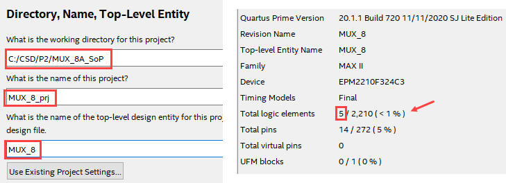 |
| Fig. 10. Project name, location and top entity. Synthesis summary. |
Synthesise your circuit and examine results. Print, analyse and comment the computer generated RTL and technology views or schematics of the circuits.
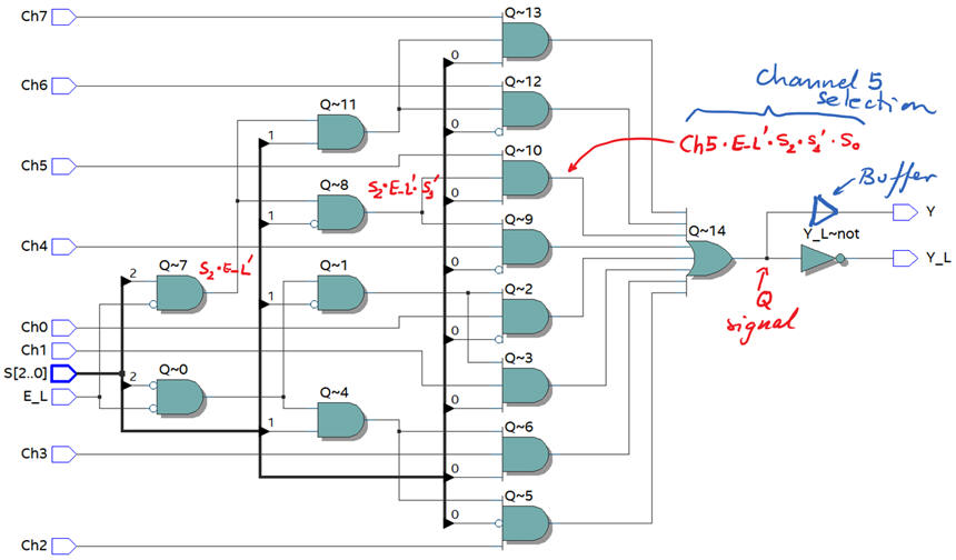 |
| Fig. 11. RTL schematic of a MUX_8 generated by Quartus Prime when using SoP equation. |
Our RTL circuit is not that different from the schematic proposed by vendors like ON Semiconductor. Chip 74HCT151 implements product terms using NAND.
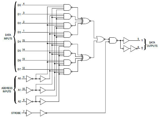 |
Fig. 12. For discussion and comparison purposes, this is the schematic of a 74HCT151 MUX_8 from ON Semiconductor datasheet. |
In Quartus Prime we can inspect how the real circuit is implemented attending the chip resources and internal architecture using technology schematic viewer and chip planner tools.
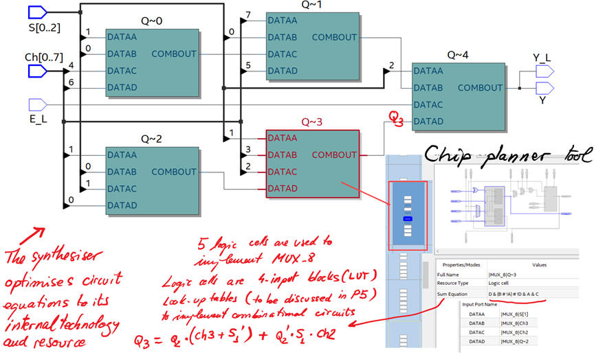 |
Fig. 13. Technology view for target chip Intel MAXII EPM2210F324C3. How many resources (logic cells) are used? |
What kind of technology contain this MAXII CPLD? For example, from MAX II 300 pages handbook (page 77) we can calculate noise margins of its input/output buffer elements (IOE). Fig. 14 shows DC characteristics of the LVTTL and LVCMOS I/O standards powered at 3.3 V.
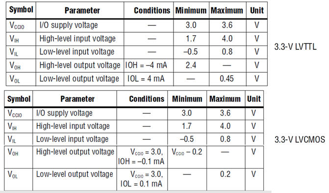 |
Fig. 14. Calculate the NMH and NML from these tables. |
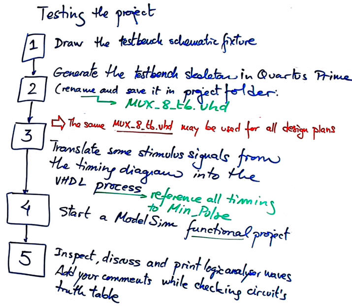
| Specifications | Planning | Developing | 4. Testing | Report | Prototype |
To test the synthesised design, whatever it is from plan A, B or C2, we use the same testbench fixture. Even if you have different internal architectures for the UUT (unit under test), the entity definition is always the same, as shown in Fig. 15, and thus the same testbench to apply stumulus can be used again.
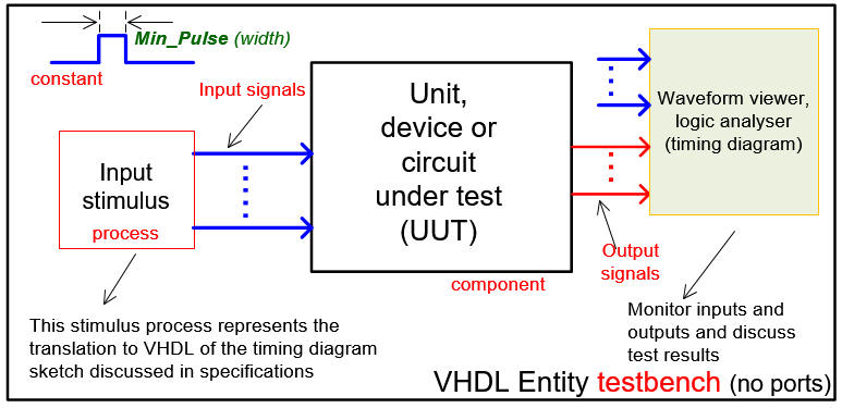 |
| Fig. 15. Testbench VHDL schematic fixture. |
Generate the template of the VHDL simulation testbench from Quartus Prime. The name of the file will be: MUX_8_tb.vhd (if the tool generates the file MUX_8.vht rename and move it into the project folder).
This is an example of testbench MUX_8_tb.vhd file representing the translation into VHDL of the schematic in Fig. 15. Waveforms in Fig. 4 are placed in "tb : PROCESS " as example stimulus.
Start an EDA VHDL functional simulation project (ModelSim) to verify the device-under-test (DUT).
Run the simulation process with only a few input vectors to see if the whole simulation process works and you are able to watch correctly input and output signals activity. Add more test vectors to verify how the information of each channel is selected.
-
What value are you choosing for Min_Pulse? How long will be necessary to run the simulation for the stimulus represented in Fig. 4?
-
How long does it take to simulate the complete truth table imagining that all stimulus vectors have the same duration 2.3*Min_Pulse?
Useful hints in ModelSim. You can order the signals as in the initial sketch in Fig. 4 for a better interpretation of the truth table and simulation result.
 |
|
Fig. 16. Order the entity input and output ports as in the initial sketch. |
You can save and restore this signal setup in a convenient wave.do file, as shown in Fig. 17, so that it can be reused in other simulations of the same entity.
The instrument setup can be saved as a convenient wave.do file in your project folder as shown in Fig. 17 and reused again for other simulations of the same entity.
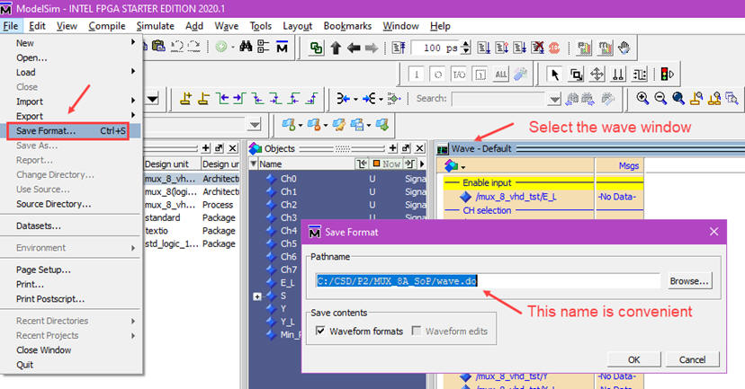 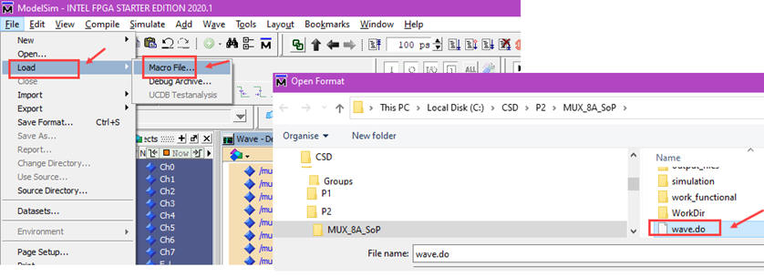 |
| Fig. 17. Save and restore the instrument setup in a txt file wave.do (its format type is TCL language). |
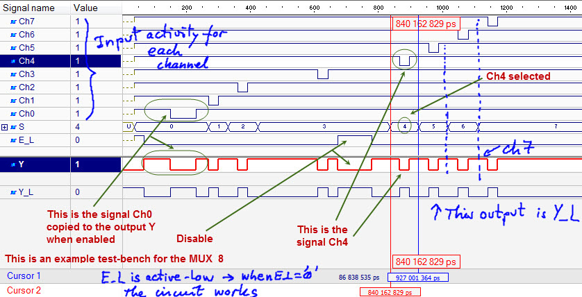
Print the timing diagram screen and add comments on the signals to show how the device works. Fig. 18 shows an example of commented test bench results from the logic analyser (wave) available in the EDA simulation tool. Use coloured pens.
 |
|
Fig. 18. Example of a timing diagram produced by the simulator with some mandatory comments and discussion on the way the circuit works. |
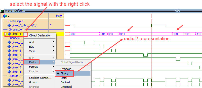
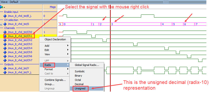
You can change the radix in which signals are represented. For instance, in this MUX_8 circuit, the vector S(2..0) can be displayed in radix-2 or in radix-10, as shwon in Fig. 19 and Fig. 20 below.
 |
|
Fig. 19. Select the signal of interest S(2..0) to change to binary radix-2 representation. |
 |
|
Fig. 20. Select the signal of interest S(2..0) to change to radix-10 (unsigned decimal). |
| Specifications | Planning | Developing | Testing | 5. Report | Prototype |
Follow this rubric for writing reports.
|
Laboratory |
Laboratory 2: designing a standard MUX_8. Flat single-file VHDL: Plan A - Plan B - Prototype This is the reference highlighted project (Hex_7seg_decoder) solved using plan B |
[3/10] |
|
Individual post lab assignment PLA2 to be discussed next Lab3. Solve and study all the details in this lab class before attempting to apply it to solve the post lab assignment. |
| 1. Specifications | Planning | Developing | Testing | Report | Prototype |
Design a MUX_8 with characteristics similar to the classic 74HCT151 chip in a programmable logic device (PLD) target chip following structural plan B using our VHDL design flow and EDA tools for developing and testing.
|
|
 |
|
|
|
| Fig. 1. Symbol and truth table. | |
In Fig. 2 there is an sketch of timing diagram.
|
|
|
Fig. 2. Example of a timing diagram sketch to demonstrate how the circuit works for different inputs. Inputs will be translated to VHDL as stimulus signals in the simulation testbench. |
| Specifications | 2. Planning | Developing | Testing | Report | Prototype |
This flowchart explains the main concepts involved in VHDL design flow process.
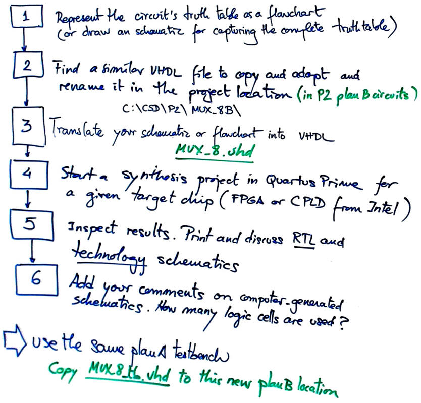 |
| Fig. 3. Plan B sequence of operations. |
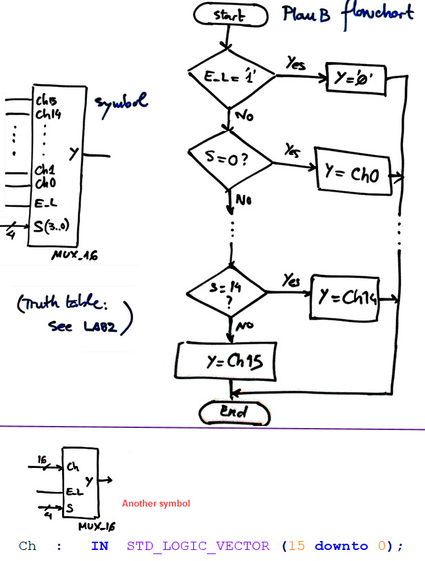
Translate the truth table into an algorithm or flowchart (rec.) or schematic for capturing the complete truth table. As shown in Fig. 4 there are always several options to obtain a flowchart.
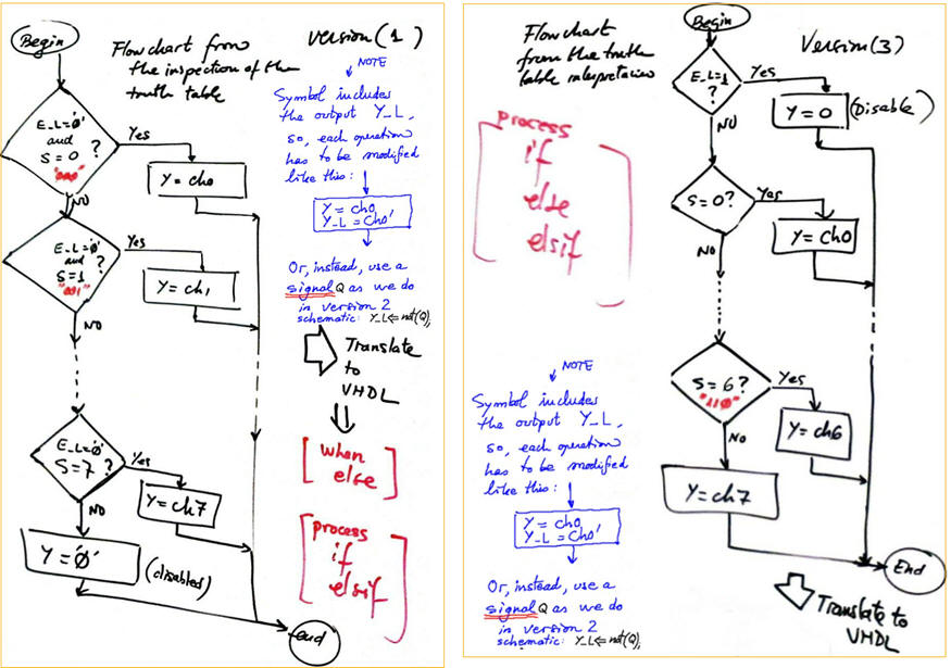 |
| Fig. 4. Plan B flowchart interpretations of the truth table, versions (1) and (3) |
And several options as well to capture the complete truth table in a single statement.
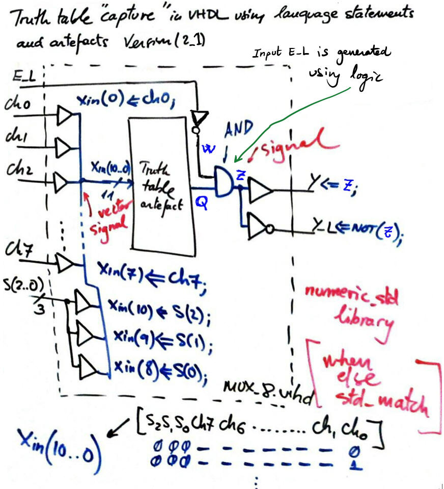 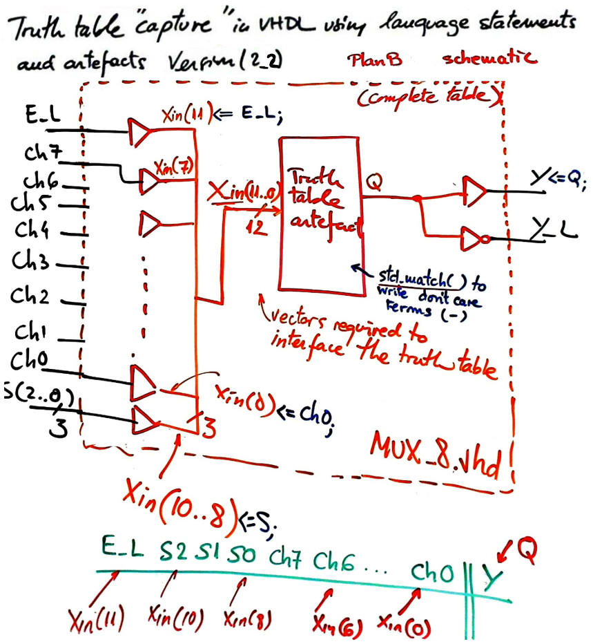 |
| Fig. 5. Plan B truth table capture, versions (2_1) and (2_2) |
Each behavioural version will generate a different VHDL file, thus, adapt folder names for saving them:
C:\CSD\P2\MUX_8B1\(files)
C:\CSD\P2\MUX_8B2_1\(files)
C:\CSD\P2\MUX_8B2_2\(files)
C:\CSD\P2\MUX_8B3\(files)
| Specifications | Planning | 3. Developing | Testing | Report | Prototype |
Find in P2 a similar circuit designed using plan B with an architecture that corresponds to a truth table or algorithm to copy and adapt.
Translate your algorithm, flow chart or schematic into VHDL in a single file. These are up to four versions: (1) MUX_8.vhd; (2_1) MUX_8.vhd; (2_2) MUX_8.vhd; (3) MUX_8.vhd, accordingly to the plans inferred above.
The entity name and VHDL description is related to the symbol in Fig. 1 and it does not depend on the plan.
|
|
| Fig. 6. The entity description in VHDL is the same for all design plans. |
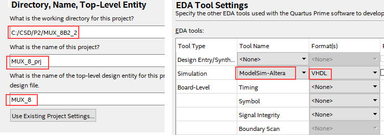
Start a new project in Quartus Prime, name it MUX_8_prj and select a target programmable chip (CPLD or FPGA) from our laboratory training boards. For instance, use Intel MAX II CPLD EPM2210F324C3, the same used above in plan A for better comparing circuit realisations.
 |
| Fig. 7. New project in Quartus Prime. |
Synthesise your circuit and examine results. Print, analyse and comment the computer generated RTL and technology views or schematics of the circuits.
 |
| Fig. 8. Example of RTL (click to expand). Why is this circuit such different from the one in plan A Fig. 11 above? |
As shown in Fig. 9, even for initial source VHDL files based on totally different plans, the same technology circuit is implemented for real in the target chip.
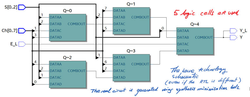 |
|
Fig. 9. Example of technology view. How many resources (logic cells) are used? How different is this circuit from the one represented in plan A Fig. 13 above? |
Discuss advantages and drawbacks of plan A and plan B.
NOTE: To show you how practical is plan B in VHDL, this is the fast adaptation of the flowchart version for a MUX_16.vhd.
| Specifications | Planning | Developing | 4. Testing | Report | Prototype |
To test the solution whatever it is from any plan, use the same test bench because even if you have invented different architectures, we use always the same entity under test. The testbench fixture containing the main ideas and concepts involved in this schematic is represented in Fig. 10.
|
|
| Fig. 10. Testbench VHDL schematic. |
Generate from Quartus Prime the testbench template in Fig. 10. Rename it and move it to the project folder. Delete the empty process.
Translate the stimulus signals into a process and set the constant Min_Pulse in Fig. 4. This is a VHDL testbench example MUX_8_tb.vhd from which you can copy only the stimulus process and Min_Pulse constant.
Start an EDA VHDL simulator project to verify the device-under-test (DUT) using the VHDL simulator test bench.
In Fig. 11 there is an example of commented test bench results from the logic analyser (wave) available in the EDA tool simulation tool. Use coloured pens.
|
|
|
Fig. 13. Example of a timing diagram produced by the simulator with some mandatory comments and discussion on the way the circuit works. |
| Specifications | Planning | Developing | Testing | 5. Report | Prototype |
Follow this rubric for writing reports.
|
Laboratory |
Laboratory 2: designing a standard MUX_8. Flat single-file VHDL Plan A - Plan B - Prototype |
[3/10] |
6. Designing an FPGA prototype
This is an example of the next step in the VHDL design flow: Choose an FPGA prototyping platform, design an extension PCB board to place the required inputs and outputs, assign pins, configure the chip, run and perform measurements using laboratory instrumentation.
| Prototype specifications | Planning | Development | Test & measurements |
To practise with multiplexers and demultiplexers, we imagine the prototype sketched in Fig. 1, a circuit MUX_DeMUX to be synthesised in a DE10-Lite board populated with an Intel MAX10 FPGA chip.
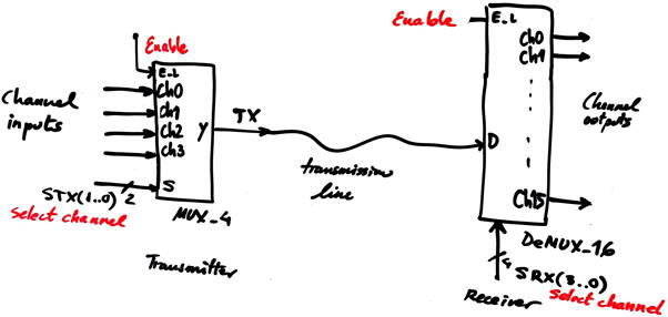 |
|
Fig. 1. MUX_DeMUX initial sketch. |
To review the theory and how the components work, we capture a Proteus schematic and run simulation models based on classic * 74LS chips: MUX_DeMUX.pdsprj. We can generate several digital signals using push-buttons, switches and even internal CLK generators. We can observe the distributed signals using an array of LED.
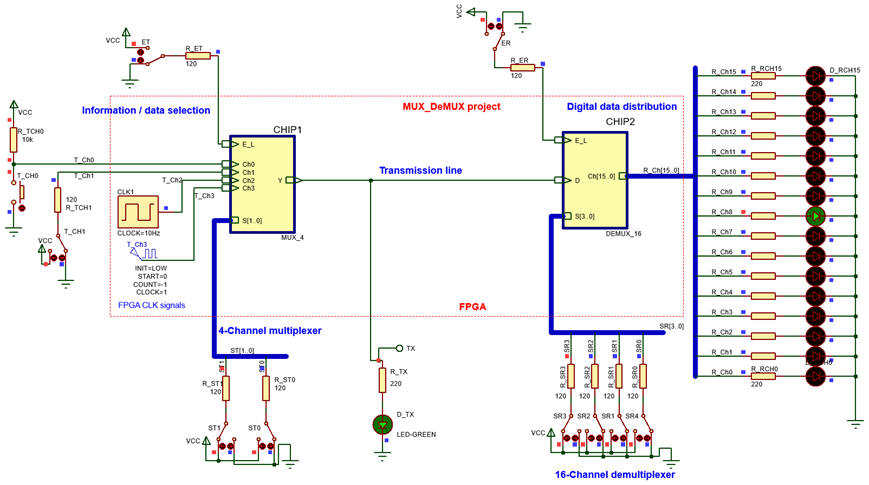 |
|
Fig. 2. Circuit captured in Proteus ready for simulation. |
| Prototype specifications | Planning | Development | Test & measurements |
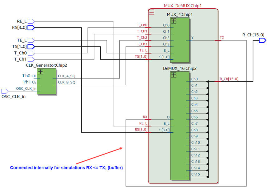
We will synthesise all the logic circuits in the target FPGA Intel MAX10 10M50DAF484C7 populating the DE10-Lite board. We can conceive the project hierarchically using Plan C2 in three levels: the standard MUX_4 and DeMUX_16 components from our libraries, the component MUX_DeMUX and the MUX_DeMUX_top including the CLK_Generator to generate a pair of channels with dynamic signals. The idea is represented in Fig. 3.
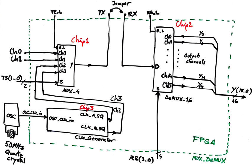 |
|
Fig. 3. Prototype plan indicating inputs, outputs and internal hierarchical architecture. On the MUX_4 side, Ch2 and Ch3 will be driven by 10 Hz and 1 Hz squared signals. |
Components:
- MUX_4 is studied in L2.1.
- DeMUX_16 is studied in L2.2.
- CLK_Generator, to be studied in L8.2 with the idea of providing two additional dynamic digital signals to multiplex.
For simulating the circuit using a ModelSin testbench, Fig. 3 is convenient. For designing the hardware prototype, TX and RX are going to be external pins to characterise the signals using laboratory instrumentation.
| Prototype specifications | Planning | Development | Test & measurements |
Printed circuit board (PCB)
In this experiment, instead of using the board's switches and LED, we can use the DE10-Lite expansion connector represented in Fig. 4, to attach a PCB with inputs and outputs. In blue colour the FPGA pins, in green colour the circuit signals.
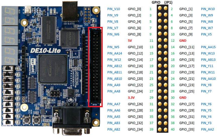 |
|
Fig. 4. DE10-Lite expansion connector assignments. |
Thus, once the hardware circuit for the PCB is conceived, we organise a KiCad project CSD_LAB2_PCB_v1.zip. The schematic can be captured as shown in Fig. 5. Each component contains the symbol, the footprint along with its 3D model, and a link to the datasheet to prepare the bill of materials (BOM) spreadsheet.
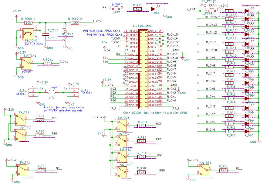 |
|
Fig. 5. Schematic captured in KiCad. We can have the same schematic annotated with different versions of component footprints and thus generate several PCB. |
The accompaning PCB component placement is shown in Fig 6.
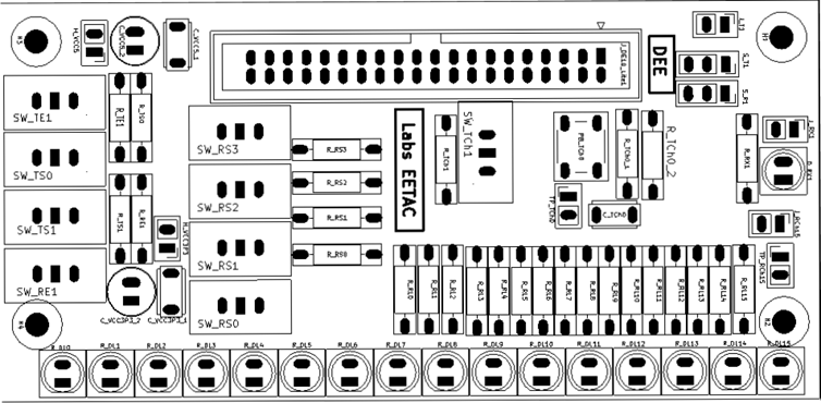 |
|
Fig. 6. PCB layout silkscreen that shows component placement and references. |
Finally, a 3D view of this PCB v1 shows the real dimensions and how the PCB will look like once soldered. If a given component fooprint 3D model is missing, KiCad works perfectly well with FreeCAD to add it to the components database.
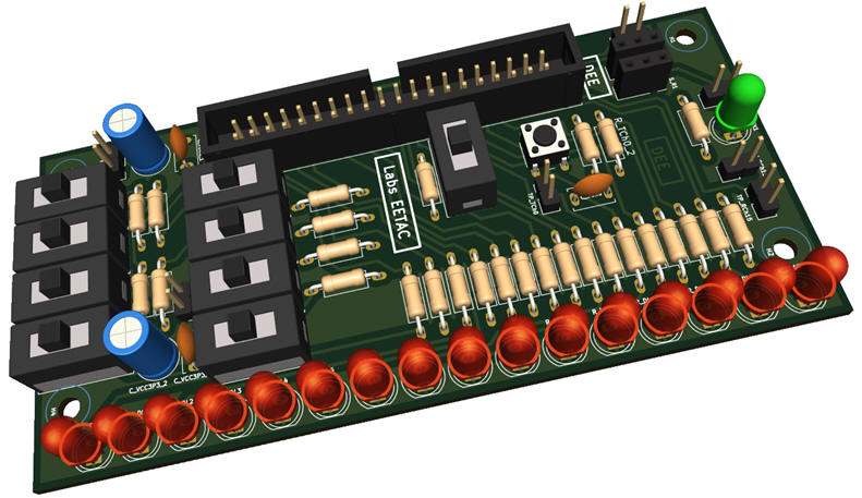 |
|
Fig. 7. PCB 3D representation. |
As an example, the green TX LED 3D model is imported into FreeCAD from the component distributor's datasheet. The pins are cut before attaching the footprint and exporting its step model.
NOTE: Current CSD and DEE KiCad symbols, footprints and 3D tuned components are available in these three libraries: symbols.zip, footprints.zip and 3dmodels.zip, to be unzipped and placed in the corresponding 3rdparty user directory. Basically, in this introductory PCB design level, the idea behind tuning components is to enlarge their pads for easy soldering.
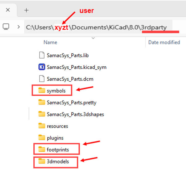 |
|
Fig. 8. KiCad custom libraries. |
FPGA circuit
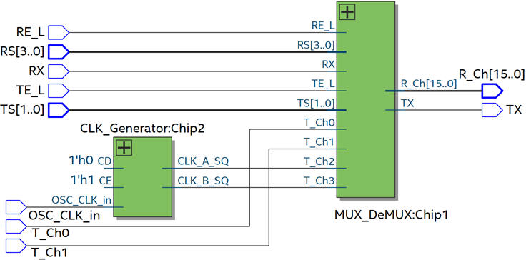
Once the board is manufactured we can configure and program the FPGA using Quartus Prime translating into VHDL the schematics in Fig. 3. For instance:
MUX_4.vhd is solved using plan A and the equation PoS. DeMUX_16.vhd is translated as plan B. The CLK generator (CLK_Generator.vhd, T_FF.vhd, freq_div_2500000.vhd, freq_div_10.vhd) and the the application MUX_DeMUX.vhd are designed using using plan C2. The top circuit for running ModelSim where TX = RX connected internally is MUX_DeMUX_top.vhd.
 |
|
Fig. 9. Synthesised top RTL for the ModelSim simulation. |
ModelSim simulation:
Using for instance this testbench MUX_DeMUX_top_tb.vhd you can perform simulations as shown in Fig. 10.
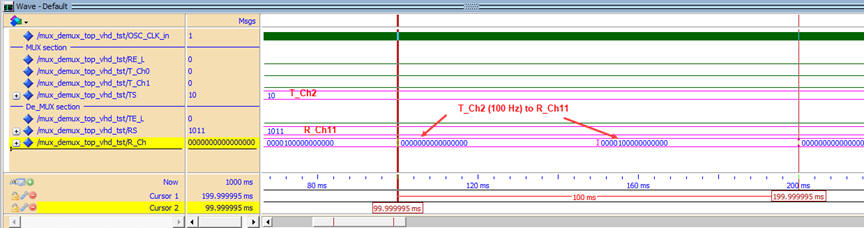 |
|
Fig. 10. Synthesised top RTL for the ModelSim simulation. |
FPGA programming:
The same top circuit for configuring the prototype where TX and RX are also external pins is MUX_DeMUX_top.vhd.
 |
|
Fig. 11. Synthesised top RTL for the prototype. |
Using the pin assignment tool as shown in Fig. 12, we can fill in all the spreadsheet and save it for later use in standard format. This is the pin assignment file MUX_DeMUX_prj.csv that can be included in the project.
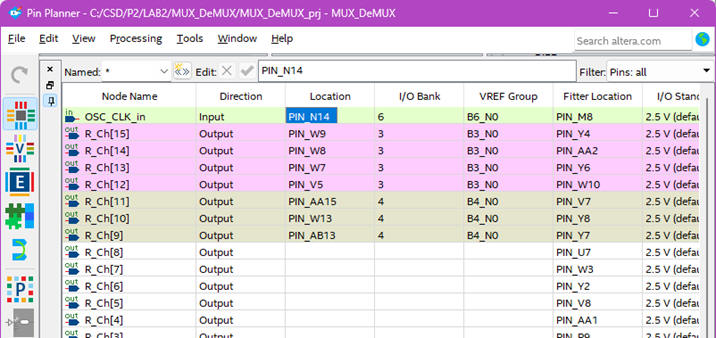 |
|
Fig. 12. Pin assignment spreadsheet. |
This is the full collection of project source files: MUX_DeMUX_top.zip.
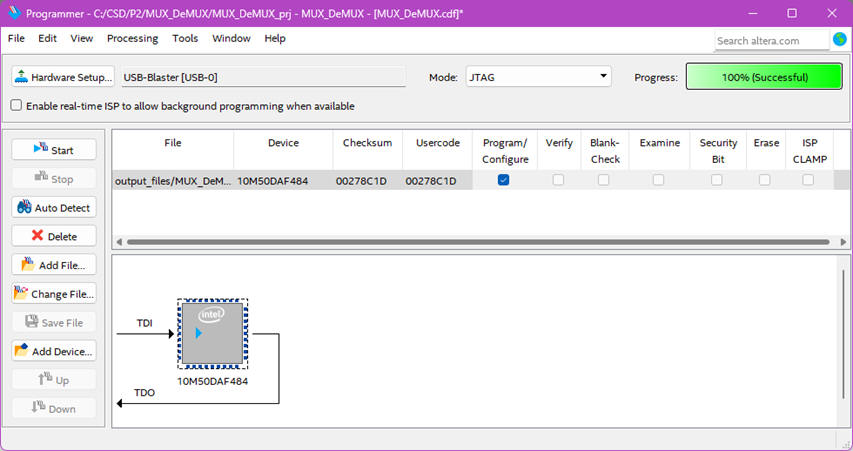
Using the Quartus Prime programmer tool (Fig. 13) we configure the FPGA in a single step. This is the file MUX_DeMUX.sof that can also be used with the programmer alone. This is the version for writing the boards memory and make the configuration permament is required: MUX_DeMUX.pof
 |
|
Fig. 13. Quartus Prime programmer configuring the FPGA for this application. |
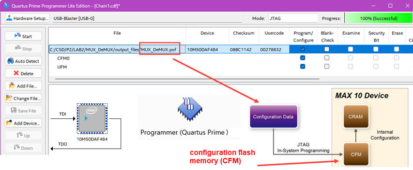
In case we like to write the configuration flash memory (CFM) of the FPGA and make the circuit permament, the programmer object file (.pof) is required: MUX_DeMUX.pof. During internal configuration, for instance on power ON, MAX 10 devices load the configuration RAM (CRAM) with configuration data from the CFM.
 |
|
Fig. 14. Quartus Prime programmer writing the flash memory (CFM) of the FPGA for this application. |
NOTE: The initial DE10-Lite default circuit can be reinstalled using this: DE10_LITE_Default.pof.
| Prototype specifications | Planning | Development | Test & measurements |
The final board prototype is represented in Fig. 15.
 |
|
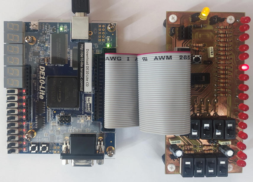
Fig. 15. Prototype connecting the inputs and outputs board to the DE10-Lite training board. |
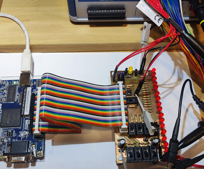
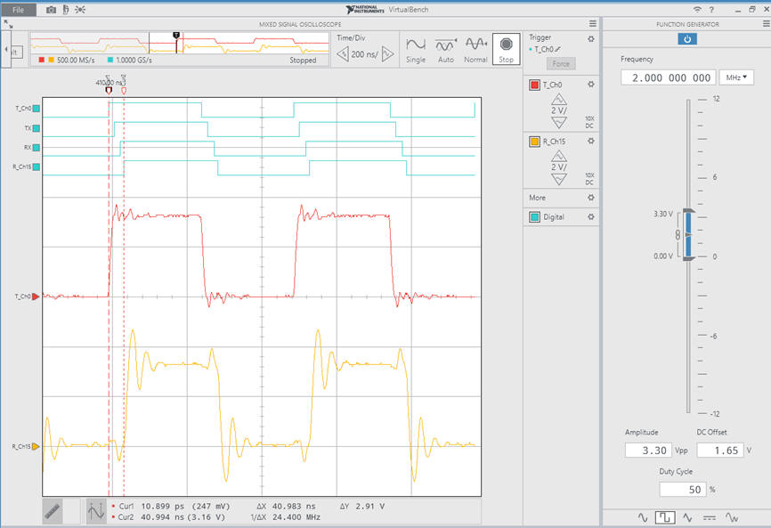
Measurement setup using the compact VB8012 instrument.
Let us apply in T_Ch0 a 2 MHz square waveform and acquire all the signals of interest: Analogue and digital versions of T_Ch0 and R_Ch15; digital signals TX and RX.
 |
|
Fig. 16. Connecting analogue and digital probes from the compact instrument |
 |
|
Fig. 17. Captured waveforms where we can measure the propagation delays among the several circuits stagrees using time cursors. Unfiltered analogue signals show ringing and coupled noise. |
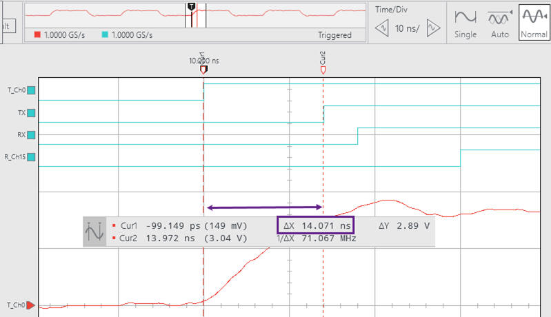
1) We can leave open the jumper J_T1 and connect the MUX_4 output TX to the DeMUX_16 input RX using a transmission line and perform measurements.
 |
|
Fig. 18. MUX_4 section propagation delay from T_Ch0 to TX. |
 |
|
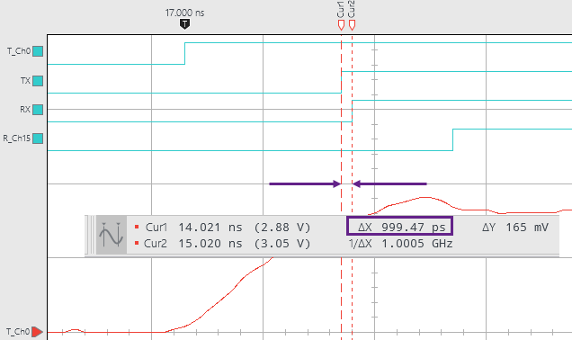
Fig. 19. The propagation delay from TX to RX using a short (1 cm) jumper is 1 ns. Well, difficult to say because the current resolution of the instrument is precisely 1 ns (1 GS/s), thus, this measurement may be wrong. A good reason for using instrumentation with more resolution, for instance the model VB-8054 offers 2 GS/s. The same measurement using a long (3 m) twisted pair wire is 15 ns. |
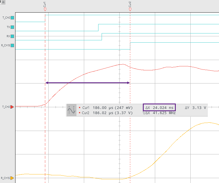
The maximum frequency of operation (in this case the applied T_Ch0 frequency) can be calculated from the measurement of the circuit total delay as in Fig. 20. fMAX < 1/(2·tP) = 20.8 MHz. You can discuss how different are these real measurements from the calculations using gate-level simulations in ModelSim. What may be the effect of the instruments bandwidth, sampling frequency and probes, PCB component placement, long flat cable from the DE10-Lite expansion connector to the PCB, etc?
 |
|
Fig. 20. Propagation delay from T_Ch0 to R_Ch15 is 24 ns. |
Other measurements of interest:
2) The two devices can also be connected using an optical fiber or IR pair (LED, photodiode).
| Home Term 24/25-Q1 Contact Products Electronic devices and companies Software Books Magazines Instruments DEE Library EETAC DEEL |

|
|
| Web activa des de 09/2001, @ F. J. Robert, J. Jordana. Web editat amb Microsoft Expression Web 4. El contingut és un complement als materials d'estudi del curs Circuits i Sistemes Digitals disponibles al campus digital Atenea. Llicència:Reconeixement 4.0 Internacional de Creative Commons |