|
|
Bachelor's Degree in Telecommunications Systems and in Network Engineering |
|
Chapter 3 problems |
- B3.14 - |
9-bit parity generator (µC - C) Dec_4_16, DeMUX_16 |
As a way to start using the new development environment (IDE) and to discover the main details of microcontroller architecture and how to program it, we can try to solve in C for a target chip PIC18F46K22 a component belonging to the 9-bit parity generator/checker proposed in D1.14 as a combination circuit.
The transmitter block contains the Parity_9bit, based only on XOR logic gates; the receiver includes the same circuit and also a simple MUX_2. On the other hand, the MUX_16 is quite similar to the Dual_MUX_4 tutorial in LAB9. Therefore, to try something slightly different and be able to practise with several inputs and outputs, we can choose between the Dec_4_16 or the DeMUX_16 circuits belonging to the channel simulator.
1.- Specifications: Dec_4_16
Design the decoder 4-to-16 represented in Fig. 1 using a PIC18F46K22 microcontroller, C language and Microchip IDE tools. Test your design using Proteus. Add switches to input signals and LED to visualise the operations.
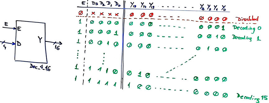 |
Fig.1. Symbol of the Dec_4_16. |
This decoder is also specified as a combinational circuit block at Dec_4_16. The emphasis is focused therefore in learning how to poll/read digital inputs and write digital outputs. The truth table will be solved using a behavioural plan B interpretation translated into C language and organising the hardware-software diagram so that the input and outputs variables will be saved in RAM memory. An infinite loop will assure the continuous calculation of the circuit's truth table.
Draw an example timing diagram.
 |
|
Fig. 2. Timing diagram example. |
2. Planning
You will solve the circuit in several steps, adding a few lines of code each time to develop and test immediately to debug any error before adding more code. For instance:
- step #1 read only E and monitor its current value var_E in a watch window.
- step #2 read the vector D(3..0) and monitor its current value in a watch window. In this way, your read_inputs() function will be validated.
- step #3 Imagine a given value for the variable var_Y (it is uint_16t) write it in the corresponding pins and observe LED values, thus validating your function write_outputs().
- step #4 complete the truth table and the project.
A) Planning hardware
Copy and adapt a circuit from any of the LAB9 projects and name it "Dec_4_16.pdsprj". Assign pins to inputs and outputs accordingly to one of the following options (your instructor will tell you which):
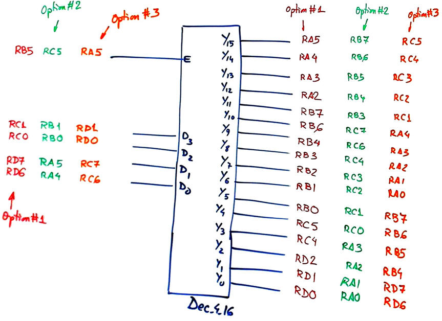
Pin assignment option #1: as indicated in the schematic above.
E --> RB5; D(3..2) ---> RC(1..0); D(1..0) ---> RD(7..6); Y(15..12) ---> RA(5..2); Y(11..10) ---> RB(7..6); Y(9..5) ---> RB(4..0); Y(4..3) ---> RC(5..4); Y(2..0) ---> RD(2..0)
Pin assignment option #2: as indicated in the schematic above.
Pin assignment option #3: as indicated in the schematic above.
Project location:
C:\CSD\P9\Dec_4_16\(files)
B) Planning software
Organise the main program in our CSD way. Copy and adapt a source code from any of the LAB9 projects and name it "Dec_4_16.c".
Propose a hardware-software diagram naming all the electrical signals, RAM variables and the software functions.
|
|
|
Fig. 3. Hardware-software diagram. |
Describe all the RAM memory variables used in this project and its type.
Explain how to configure the µC in init_system().
Organise using a flowchart the interface function read_inputs().
|
|
|
Fig. 4. Reading inputs. |
Organise using a flowchart the interface function write_outputs().
|
|
|
Fig. 5. Writing outputs. |
Infer the truth_table() software function using a behavioural plan B interpretation from the corresponding flowchart.
|
|
|
Fig. 6. Dec_4_16 initial discussion on adapting the truth table using plan B flowcharts. |
3. Developing & 4. Testing (debugging)
- Step #1. Write the "Dec_4_16.c" source code translating the function flowcharts. Start capturing only one input as in (LAB9) and visualising it in the watch window as a RAM variable as indicated in the sequence of steps above in the planning section. And, only then go to the next step developing & testing more inputs.
Start a software IDE project for the target microcontroller PIC18F46K22 and generate the configuration files ".cof" and ".hex" after compilation. Discuss the project summary: % of ROM used for the code, number of RAM bytes used, etc.
| Note: Step-by-step tactical approach for developing and testing the project: Read one input at a time and run to check that the voltage value is correctly captured as a valid digital value in RAM memory. Write one output at a time and run to check that your code is correct to light the LED connected at the output pin. |
Add a few lines of code every time, compile and run the test interactively to check results watching variables.
|
|
|
Fig. 7. Example pictures demonstrating how the circuit works. |
Measure how long does it take to run the main loop code when using a 4 MHz and a 16 MHz quartz crystal oscillator. Thus, how many times per second is calculated the circuit's truth table?
|
|
|
Fig. 8. Loop execution time measurements. |
1.- Specifications: DeMUX_16
Design the 16-channel demultiplexer represented in Fig. 1 using a PIC18F46K22 microcontroller, C language and Microchip IDE tools. Test your design using Proteus. Add switches to input signals and LED to visualise the operations.
 |
Fig.1. Symbol of the DeMUX_16. |
This demultiplexer is also specified as a combinational circuit block at DeMUX_16. The emphasis is focused therefore in learning how to poll/read digital inputs and write digital outputs. The truth table will be solved using a behavioural plan B interpretation translated into C language and organising the hardware-software diagram so that the input and outputs variables will be saved in RAM memory. An infinite loop will assure the continuous calculation of the circuit's truth table.
Draw an example timing diagram.
|
|
|
Fig. 2. Timing diagram example. |
2. Planning
You will solve the circuit in several steps, adding a few lines of code each time to develop and test immediately to debug any error before adding more code. For instance:
- step #1: Read only E_L and monitor its current value var_E in a watch window.
- step #2: Read the vector S(3..0) and monitor its current value in a watch window. In this way, your read_inputs() function will be validated.
- step #3: Imagine a given value for the variable var_Ch (it is uint_16t), write it in the corresponding pins and observe LED values, thus validating your function write_outputs().
- step #4: Complete the truth table and the project.
A) Planning hardware
Copy and adapt a circuit from any of the LAB9 projects and name it "DeMUX_16.pdsprj". Assign pins to inputs and outputs accordingly to one of the following options (your instructor will tell you which):
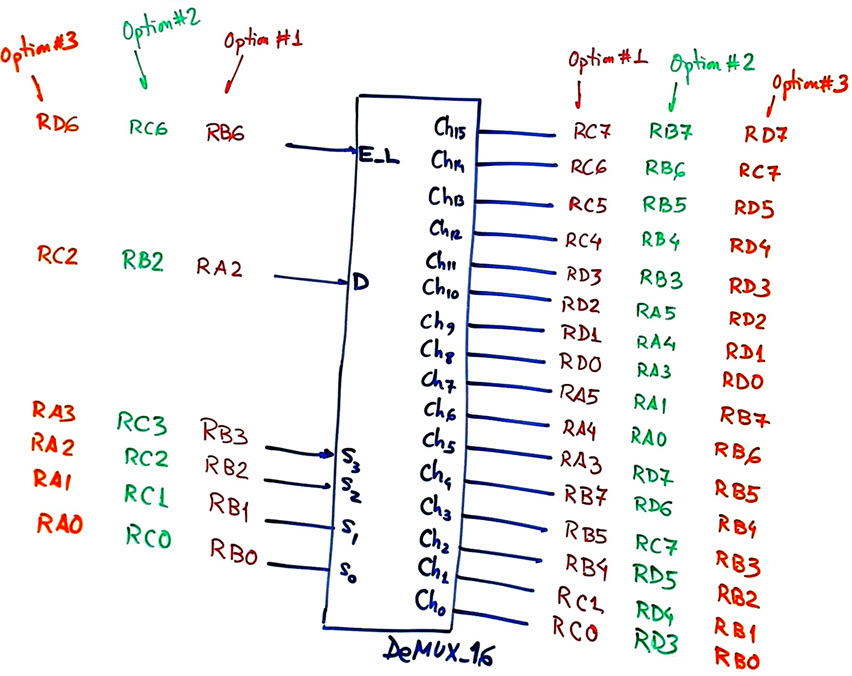
Pin assignment option #1: as indicated in the schematic above.
E_L --> RB6; D ---> RA2; S(3..0) ---> RB(3..0); Ch(15..12) ---> RC(7..4); Ch(11..8) ---> RD(3..0); Ch(7..5) ---> RA(5..3); Ch(4..2) ---> RB(7..4); Ch(1..0) ---> RC(1..0)
Pin assignment option #2: as indicated in the schematic above.
Pin assignment option #3: as indicated in the schematic above.
Project location:
C:\CSD\P9\DeMUX_16\(files)
B) Planning software
Organise the main program in our CSD way. Copy and adapt a source code from any of the LAB9 projects and name it "DeMUX_16.c".
Propose a hardware-software diagram naming all the electrical signals, RAM variables and the software functions.
|
|
|
Fig. 3. Hardware-software diagram. |
Describe all the RAM memory variables used in this project and its type.
Explain how to configure the µC in init_system().
Organise using a flowchart the interface function read_inputs().
|
|
|
Fig. 4. Reading inputs. |
Organise using a flowchart the interface function write_outputs().
|
|
|
Fig. 5. Writing outputs. |
Infer the truth_table() software function using a behavioural plan B interpretation from the corresponding flowchart.
|
|
|
Fig. 6. Dec_4_16 initial discussion on adapting the truth table using plan B flowcharts. |
3. Developing & 4. Testing (debugging)
- Step #1. Write the "DeMUX_16.c" source code translating the function flowcharts. Start capturing only one input as in (LAB9) and visualising it in the watch window as a RAM variable as indicated in the sequence of steps above in the planning section. And, only then go to the next step developing & testing more inputs.
Start a software IDE project for the target microcontroller PIC18F46K22 and generate the configuration files ".cof" and ".hex" after compilation. Discuss the project summary: % of ROM used for the code, number of RAM bytes used, etc.
| Note: Step-by-step tactical approach for developing and testing the project: Read one input at a time and run to check that the voltage value is correctly captured as a valid digital value in RAM memory. Write one output at a time and run to check that your code is correct to light the LED connected at the output pin. |
Add a few lines of code every time, compile and run the test interactively to check results watching variables.
|
|
|
Fig. 7. Example pictures demonstrating how the circuit works. |
Measure how long does it take to run the main loop code when using a 4 MHz and a 16 MHz quartz crystal oscillator. Thus, how many times per second is calculated the circuit's truth table?
|
|
|
Fig. 8. Loop execution time measurements. |
| Home Term 26/27-Q1 Contact Products Electronic devices and companies Software Books Magazines Instruments DEE Library EETAC DEEL |

|
|
| Web activa des de 09/2001, @ F. J. Robert, Web editat amb Microsoft Expression Web 4. El contingut és un complement als materials d'estudi del curs Circuits i Sistemes Digitals disponibles al campus digital Atenea. Llicència:Reconeixement 4.0 Internacional de Creative Commons |