|
|
Bachelor's Degree in Telecommunications Systems and in Network Engineering |
|
|
| |||
|
|
P_Ch2 Questions and answers. Programmable timer (Prog_Timer) |
|
|
| |||
Question: I have a doubt: as we must compare the electrical parameters of the chip implemented in 2 different target chips, shall we create 2 different whole projects for each one? Because just at the really first step, at the Quartus Prime project�€™s creation, we need to specify the target chip that we are using to implement the chip. So I guess we need to take into account 2 whole different projects, and thus, different folders for each target chip, right?
Answer: If you are inventing two different architectures, you require two projects in separated folders. If you are simply selecting between two chips, one project in one folder is ok. Simply re-synthesise and re-run the simulation gate-level and the timing analyser to observe and measure propagation times. Probably, the same design targeted for two technologies will generate different propagation delays and maximum speed of computing.
Question: I'm trying to do the test part for the SP2_1, I've already done all the vhd files without any error so I can run the project and see the RTL viewer and more. So now I am doing the following step and I can't do it because I always receive error meassgess messages. Even though I tried to fix it always appears when I want to run the gate-level.
Answer: This SP2_1 consist of two parts: (1) learning how to use the new tools, (2) inventing a new circuit and apply the new tools for making measurements and discussing results.
For solving (1), you have to run and complete the LAB4 experiments (up to two/three projects) and also the additional project in this unit on basics on gate-level measurements. You may also ask us any question about it, no problem, we regularly improve such tutorials and experiments from your direct feedback.
For solving (2), it is only about repeating another time what you have learnt in previous tutorials, so, no errors on files, folders, etc, but simply questions about the schematic in plan C2 that you are inventing.
Question:Once we have developed the project with the CYCLONE IV, and we move on to develop it with the MAX II, how do we name the project when we open Quartus? Do we keep the same name or can we change it?
Answer: As the tutorial in LAB4 explains, if you are changing only the chip, do not implement a new project, but modify this parameter "Device..." and re-synthesise it again and re-compile and restart for new measurements for comparisons in chip performances and further discussion. If you are changing the architecture of a circuit (for instance from an Adder_4bit using ripple-carry to an Adder_4bit using carry-look ahead) you have to implement another project. Follow LAB4 project Adder_10bit indications.
Question: How to organise the project and write the report?
Answer: These are some ideas:

Question: For method 3, do we have to test the MAX and the Cyclone chips or only one of them?
Answer: One chip is ok. The idea of gate-level VHDL here is to observe and measure, as in LAB5 Fig. 15, the parameter propagation time CLK to output (tCO). And also run the timing analyser tool to observe how complicated (or useless) it is when several CLK signals are identified.
Question: In method 1, in the planning, we have to draw the timing diagram. So in the development what should we put? Because in digsys there are only development points for plans C,D and E.
Answer: General 1-2-3-4 report organisation do not apply for certain simple analysis or designs. For example designing a canonical circuit using maxterms is immediate because the circuit itself is the truth table equation, thus 2-3 is simply drawing the circuit. If you have to analyse the circuit using method 1 to deduce its timing diagram and what the circuit is for, tools are simply pen & paper. The plan and development (2-3) may be 1] solve a circuit with one T_FF, and 2] solve the circuit with all three T_FF. Section 4 on testing may be a simple sentence, solved by results comparison once you have got results from other methods.
Question: In the SP2_2 all the chips are sensitive to the falling edges of the clock signals or it is just for the chip circled in red in the picture?

Answer: I see that all the chips have the same symbol. The first thing here for you is to redraw your circuit in paper, simply to make clear all circuit connections and components. This picture is from a book, so this is what I did, draw it again myself accordingly to our conventions, so that before any analysis attempt, it will look like any other CSD circuit.
Question: How to organise the project and write the report?
I have a question about SP2_2 assignment of CSD. Do we have to make 3 reports (one per method, 3 stacks of sheets) or can we make 1 report for all 3 methods (only 1 stack of sheets)?
Answer: These are some ideas: Do this assigment only after having solved LAB5. Between 8 and 12 sheets (because 1-1-1 and 4-4-4 are pretty much the same sheet) (as it was in analysisi SP1_1). I have a question about SP2_2 assignment of CSD. Do we have to make 3 reports (one per method, 3 stacks of sheets) or can we make 1 report for all 3 methods (only 1 stack of sheets)?

This is an analysis problem, like P1 and SP1_1 or SP1_2, where several methods with different tools are used for deducing the solution. So, it is necessary to organise one report 1-2-3-4 for each method. Write down and draw one time the specifications (step 1) and photocopy them two times. Then, follow the three paths (steps 2-3) independently using different folder locations and etc. Finally, step 4 is simply a solution comparison and final discussion, so one time is ok indicating that the two/three methods give you the same solution. The idea is that from such experiments you can learn how to solve similar exam EX2 problems.
Solving similar circuits using method 1 from P5 section or from exams is recommended for fully comprehending how FF works.
Question: How to represent current_state and next_state FSM signals in a wave diagram as represented in this picture?
Answer: For example, in this video rec. attached to the specifications that explain how P6 on matrix keyboard is designed. At time 1:50:00 more or less, it is explained how to add current_state and next_state to the final wave diagram in functional VHDL simulations, to get a clearer picture on how the FSM works in time. Observe how current_state is synchronous with the CLK's rising edge. Be aware that such internal signals are not that easily available in gate-level simulations where you are testing the vho technology schematic synthesised by Quartus Prime (what can be done to visualise internal states also when simulating technology schematics?).
Question: I was studying and doing some sample questionnaires and I do not understand how is the Gray coding when we want to design the control unit for an asynchronous serial data receiver dedicated processor. It has 10 states. In one-hot we need 10 D_FF and in binary we need 4 D_FF. But in Gray I do not know how to solve it.
Answer: You are right, if your state diagram has 10 states ---> 10 labels to save in the internal state register as combinations of ones and zeros. One-hot encoding of the 10 labels ---> 10 D_FF; binary sequential (radix-2) --> 4 D_FF; Gray code --> 4 D_FF, because even if the combinations are ordered differently than in radix-2, you also have 16 different combinations and only 10 of them will be used.
You can set the codes Quartus Prime will assign to your FSM, there is a compiler (synthesiser) option to choose this internal code for present_state (click images to view):


Question: I have a doubt about the report of SP2_4, it needs 4 sheets for datapath and discussing Counter_mod16M and Data_reg24bit or we need 4 sheets for each Chip1, Chip3 and Datapath?
Answer: As a general rule, chips that you need for your design already found in digsys as sample projects do not have to be included in documents as projects, because they are fully reported, ready for new designs. All other circuits that you invent have to be included in reports.
SP2_4 is for inventing the internal architecture of the Datapath component in P_Ch2. So it is an annex in P_Ch2 report, as it is SP2_1 (component Comp_24bit) and SP2_3 (Control_unit).
SP2_4 testing (section 4) is not required, but the other 3 sections of the components Counter_mod16M and Data_reg24bit are necessary because you have to obtain these set of VHDL files in order to complete P_Ch2, right?
Sometimes, testing a Datapath alone as a separated project is complicated because you have to supply all the stimulus generated synchronously and automatically by the control unit, thus, it is better to test the final project with all the components while watching internal variables for debugging purposes until it operates as specified.
Question: How the projects in this P_Ch2 assigment are organised?
Answer: Datapath schematic planning:

Question: I have a question about the Datapath (SP2_4) component Counter_mod16M. I don't really know if the chip is supposed to be restricted to a maximum of 16 million operations per second (16 MHz) or it is supposed to be able to do a maximum of 16777216 operations per second (2^24).
Answer: For example, a Counter_mod16 counts 16 states (or numbers or different binary combinations). If its CLK is 1 Hz, it does 1 operation/second. If its CLK is 1 MHz it does 1 million operations per second. Counter modulo or counting capacity is not related to speed of computing, the later depends on the circuit technology (delay when propagating signals from inputs to outputs). We try to measure or find always the CLK to output (tCO) worst-case scenario that corresponds with the longest propagation delay, and so, the CLK's maximum period cannot be sorter that this value.
Question: Since the inputs Din and the output Q are vectors of 24 bits, I know that the minimum value will be 24 zeros (0000 0000 0000 0000 0000 0000). However, I am not sure if the maximum value will be 24 ones (1111 1111 1111 1111 1111 1111) which corresponds to the number 16777216 in radix 10 or the maximum value will be 15999999 in radix 10 (which is 1111 0100 0010 0011 1111 1111 in radix 2).
Answer: You only have to study in detail what we did in Lab7 or in other planY components, and adapt it to your project. Constant Max_Count is the last state. If you have a Counter_mod32, the last state is 31 ("11111"), if you have a Counter_mod16M (2^16 -1 is the last state). We name the circuit Counter_mod16M instead of Counter_mod16777216 simply to shorten the name and agree with what is commonly used in our digital world, for instance in memory capacity: 1 kB = 1024 Bytes, 128 MB = 134217728 Bytes.
Question:
Answer:
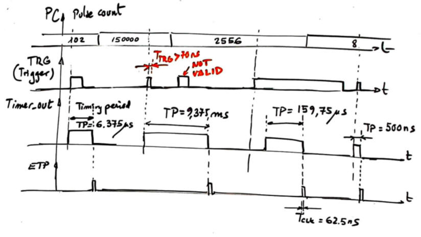
P_Ch2: Designing sequential systems: programmable timer
Question: How to write the testbench for the Prog_Timer?
Answer: Firstly, draw your timing diagram in paper as we did for instance in Fig. 2 immediately below the symbol. Think what are you going to do with input signals for the complete Prog_Timer in time to demonstrate that it works. Do not forget that your VHDL testbench with stimulus is ONLY a translation of such handwritten timing diagram. Prepare your CLK, prepare your CD pulse, prepare your PC value, and finally prepare your TRG pulse, and infer and discuss what is going to happen with circuit outputs as long as time is advancing.
Secondly, get the testbench skeleton for the Prog_Timer from Quartus Prime and draw the testbench fixture, something like this picture below, in this way you know in advance always what is going on and what you are expecting from VHDL simulations:

Thirdly, translate your inputs signals in VHDL processes (one at a time if you like) the same way we do all the time and run a functional simulation. Is your result pretty much like your timing diagram?
Question: How to prepare the video recording?
Answer: The idea of video recording is that you organise a 10 min. max. presentation in group to discuss P_Ch2 as a wholeand in the way you like. In this time slot, is also possible and adequate to discuss about collateral work (components or subprojects).
Video presentations are for audiences who may not have an idea of all project details, so, the best presentations try to explain firstly what is the top project (specifications), how it is designed (plannig), developed and tested. In subsequent slides, smaller parts and details can also be presented. Remember to leave some time for conclusions and final remarks.
Question: How to prepare the project report?
Answer: You write the P_Ch2 report in the same way as it was P_Ch1. You discuss specs/plan/development/test and conclusions of the complete P_Ch2. Attach annexes for improvements (if you have done additional work) in SP2_1, SP2_2 and SP2_3 that were already submitted individually, and another annex with the SP_2_4 report that is submitted for the first time.
Question:
Answer:
| Home Term 23/24-Q2 Contact Products Electronic devices and companies Software Books Magazines Instruments DEE Library EETAC DEEL |

|
|
| Web activa des de 09/2001, @ F. J. Robert, J. Jordana. Web editat amb Microsoft Expression Web 4. El contingut és un complement als materials d'estudi del curs Circuits i Sistemes Digitals disponibles al campus digital Atenea. Llicència:Reconeixement 4.0 Internacional de Creative Commons |