|
|
Bachelor's Degree in Telecommunications Systems and in Network Engineering |
|
|
|
|||||
Chapter 3 problems |
- D3.20 - |
5-bit Johnson counter (μC - C) |
|||
|
|
|||||
1. Specifications
To see an example of microcontroller flexibility for designing digital circuits, let us infer the classic chip 74HC4017, a Johnson decade counter. Target chip PIC18F4520 and Microchip IDE tools (MPLABX - XC8).
The same project designed using hardware is stated in D2.20.
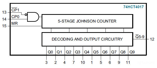 |
Fig. 1. Internal structure of the chip implemented by NXP. |
Let us add and define the new features stated in Fig. 2.
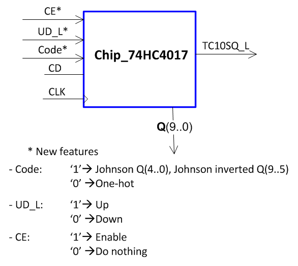 |
Fig. 2. Symbol adapted to our naming conventions and description of the chip functionality (Visio). |
Here you are some notes on specifications and planning.
Determine the execution speed. How long does it take to run a loop? And therefore, what is the maximum CLK frequency you should apply in order to make it run correctly?
2. Planning (plan X)
Fig. 3 shows an example of state diagram. This unit explains the key concept of interrupt.
We will use plan X enumerating all states.
 |
| Fig. 3. State diagram. |
You can approach the problem in successive steps. For instance:
- Step 1: plan, design and test completely a 10-bit Johnson up counter with counter enable (CE) control signal.
- Step 2: copy your previous project source files in a new folder and add the feature up/down (UD_L) to make the device reversible.
- Step 3: copy your previous project source files in a new folder and add the output combinational function to translate Johnson to one-hot code (control signal Code).
For any design step, firstly plan the hardware and secondly the software as we usually do to solve microcontroller applications.
1.- Hardware circuits and port connexions. Simply use some of the unconnected port pins available on the board to attach inputs and outputs.
2. - Software organisation. Modify the functions init_system(), output_logic(), state_logic(), read_inputs(), write_outputs(), etc. as necessary. Some notes.
RAM variables, output_logic() , state_logic() , ISR(), etc.
These Chip_74HC4017.pdsprj Chip_74HC4017.c are files to help you in this design, basically they are the project solved for a PIC16F877A: Thus an adaptation to the new target μC is required.
3. Development and 4. Testing
For any design step, compile and run Proteus and test the circuit using step by step, break points and the watch window tools. Fig. 4 show the kind of waveforms expected.
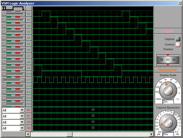 |
| Fig. 4. Example output from Proteus logic analyser instrument (CE = 1; UD_L = 1; Code = 0) |
5. Report
Follow this rubric for writing reports.
6. Prototyping
Use training boards and perform laboratory measurements to verify how the circuit works. Fig. 5 is a picture of the project under development using the PICDEM2+ board. Using Microchip ICD2 InCircuit Debugger device you can program the HEX file or debug using the COF file, as you did in Proteus.
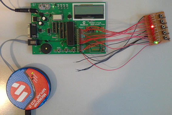 |
Fig. 5. Circuit prototype mounted in a PICDEM2+ board. |
| Home Term 24/25-Q1 Contact Products Electronic devices and companies Software Books Magazines Instruments DEE Library EETAC DEEL |

|
|
| Web activa des de 09/2001, @ F. J. Robert, J. Jordana. Web editat amb Microsoft Expression Web 4. El contingut és un complement als materials d'estudi del curs Circuits i Sistemes Digitals disponibles al campus digital Atenea. Llicència:Reconeixement 4.0 Internacional de Creative Commons |