|
|
Bachelor's Degree in Telecommunications Systems and in Network Engineering |
|
|
|
|||||
Chapter 2 problems |
- D2.20 - |
5-bit Johnson counter (FPGA-VHDL) |
|||
|
|
|||||
1. Specifications
Replicating the functionality of obsolete chips when they are required for some applications is always possible targeting programmable devices like FPGA or CPLD. Let us infer the classic chip 74HC4017 represented in Fig. 1, a Johnson decade counte, using VHDL and EDA tools from Intel such Quartus Prime and ModelSim Intel edition. target chip may be a Cyclone IV FPGA.
The same project designed programming a μC is in D3.20.
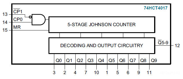 |
Fig. 1. Internal structure of the chip implemented by NXP. |
Let us add and define the new features stated in Fig. 2.
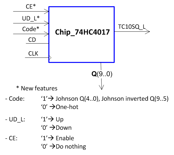 |
Fig. 2. Symbol adapted to our naming conventions and description of the chip functionality (Visio). |
Even if the schematic in Fig. 1 is is indicating an internal architecture based on several internal blocks (plan C2), you can use also plan A and plan B to solve this problem and compare circuit realisations and their respective performance.
Determine the maximum execution speed for the given target chip.
To make it easy, you can approach the problem in successive steps. For instance:
- Step 1: plan, design and test completely a 10-bit one-hot up counter with counter enable (CE) control signal.
- Step 2: copy your previous project source files in a new folder and add the feature up/down (UD_L) to make the device reversible.
- Step 3: copy your previous project source files in a new folder and add the output combinational function to translate Johnson to one-hot code (control signal Code).
| Home Term 24/25-Q1 Contact Products Electronic devices and companies Software Books Magazines Instruments DEE Library EETAC DEEL |

|
|
| Web activa des de 09/2001, @ F. J. Robert, J. Jordana. Web editat amb Microsoft Expression Web 4. El contingut és un complement als materials d'estudi del curs Circuits i Sistemes Digitals disponibles al campus digital Atenea. Llicència:Reconeixement 4.0 Internacional de Creative Commons |