|
|
Bachelor's Degree in Telecommunications Systems and in Network Engineering |
|
|
|
|||||
Chapter 2 problems |
- D2.21 - |
Programmable timer |
|||
|
|
|||||
1. Specifications
(under revision)
Design a programmable timer using the dedicated processor strategy containing datapath circuits for performing timing operations and control unit ( FSM) to sequence the process.
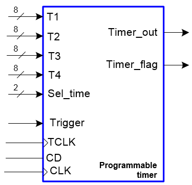 |
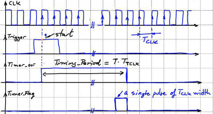
Fig 1. Programmable timer symbol (Visio) and a sketch on how it has to work. The number T is T1 or T2 or T3 or T4 depending on the Sel_time input. Therefore, counting time means counting pulses or TCLK periods (the time base) which have a vey well known and stable frequency. Generally, this TCLK signal is derived from quartz crystal using CLK generator circuits. The sysem runs synchronised to CLK. |
 |
|
- 8-bit data to program the timing period.
- Four programmable timing periods: T1, T2, T3 and T4.
- Trigger signal to start the timing period. Non-retriggerable device.
- Timer_out signal goes high while timing.
- Timer_flag signal goes high to indicate the end of the timing period, thus allowing expandability connecting this signal to the Trigger input of the next device.
- Dedicated processor design strategy.
2. Planning
Some ideas and files to start the project:
These are the initial ideas and in Fig. 2 there is the general architecture of a dedicated processor that we'll adapt to this problem. External inputs and status signals from the datapath establish the next state to go.
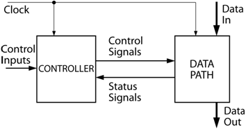 |
Fig. 2. General architecture of a dedicated processor where the control unit or controller is a FSM that handles the circuits in the datapath which are in charge of processing information. |
- Draw the state diagram of the Timer_FSM.vhd and infer the number of registers required in this project.
- Solve the Timer_FSM.vhd component:
- Adjust the general FSM topology to this problem. To which block (CC1, CC2, state register) is connected every input and output?. How many r bits are required for coding the current and next state signals [r = number of states if one-hot; r = (1/log 2)·log (number of states) if binary or Gray]
- Deduce the truth table of the CC1 and CC2 and their corresponding flow charts.
- Write the VHDL code of the finite state machine adapting an example from our web.
- Develop the Octuple_MUX4.vhd required to select the time period.
- Develop the 8-bit down counter with parallel input. Counter_8bit.vhd
- Develop the data registers. Data_register_8bit.vhd
- Optional component: Exact timing using an arithmetic circuit to offset the FSM overhead bits (adder or substractor from P4).
- Connect all the components (Counter_8bit.vhd, Octuple_MUX4.vhd, Adder_8bit.vhd, Data_register_8bit.vhd) together in the top Programmable_timer.vhd, file and implement and test the system using the Programmable_timer.vht.
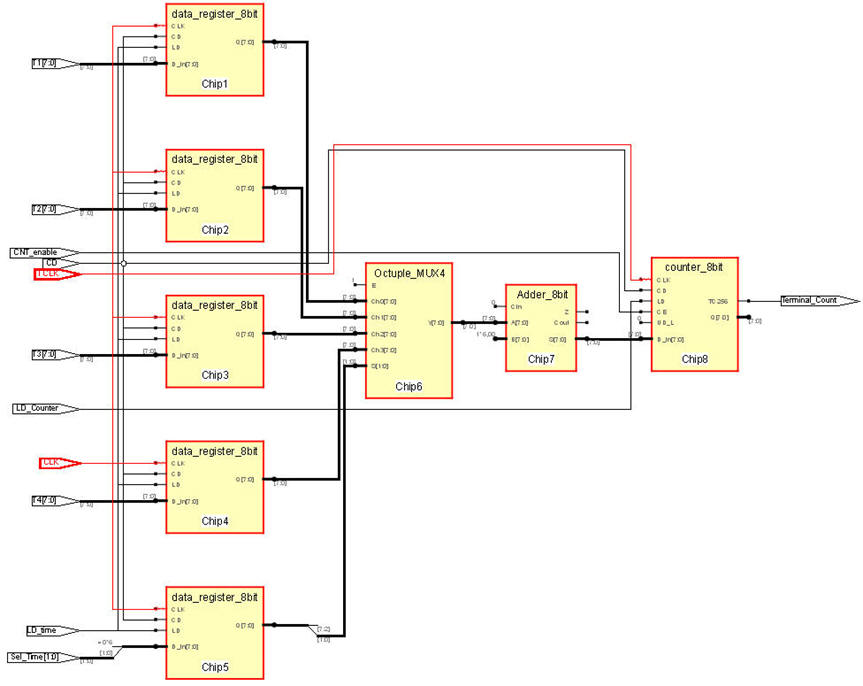
- Some files to start this plan C2 project. Adder_8bit was studied in Lab3. The top schematic is given, but some components with their empty architectures are yet to be designed. Thus, the point is that all the files included in the project can now be compiled together and the EDA tool generates the top level RTL schematic represented in Fig 3.
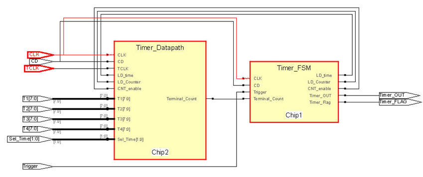 |
| Fig. 3. The top RTL view where all the components are
connected. |
NOTE: the synthesiser shows you this error because some components are not finished.

 |
| Fig. 4. The internal datapath structure. |
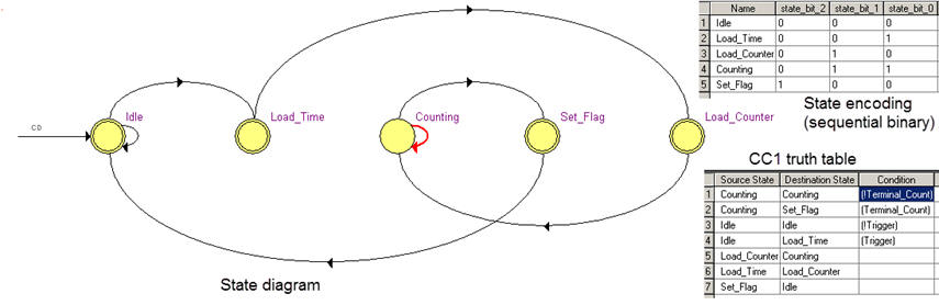 |
| Fig. 5. The timer FSM that controls the sequence of operations to be solved by the datapath. |
- Run the EDA tool to synthesise the circuit and print and comment the RTL schematic.
- Check the number of registers (D_FF) used in the target chip and justify the value. Does it match with your initial value?
- Start the test bench template and add the CLK and inputs activity translating the timing diagram. Make all the timing relative to the CLK_Period constant.
- Complete the template testbench file named Programmable_timer.vht translating a timing diagram like the one represented above in the specifications into CLK and input signals stimulus processes.
- Functional simulation. Run the EDA VHDL tool and demonstrate how the circuit works adding comments to the printed sheet of paper containing the waveforms. Your system may works like the timing diagram discussed in class.
- Run the gate-level simulation of the project and measure the maximum frequency of operation. It is worth to know exactly which is the maxim CLK frequency for a given target CPLD or FPGA chip.
|
|
|||||
Chapter 2 problems |
- D2.21 - |
Programmable timer (version 2) |
D2.22 |
||
|
|
|||||
1. Specifications
(under revision)
Let us interface the Programmable_timer developed above and the registered 16-key matrix encoder in D2.15 to generate a keypad-controlled programmable timer.
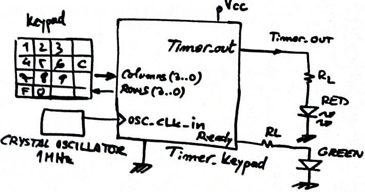 |
Fig 1. Symbol and electrical schematic for the proposed keypad-controlled programmable timer. |
- Solve the CLK generator chip to generate 100 kHz (SCLK), 200 Hz (MCLK) and the time base signal of 1 Hz from the crystal quartz oscillator available in the training board. For instance, 25.175 MHz in Altera's UP2, 50 MHz in Digilent NESYS 2 board or 1 MHz CLK signal in HWD-LC4128V from Lattice Semiconductor.
- Organise the system architecture to read T1 time from the keypad (maximum time is 99 s) and trigger the timer when clicking the key '*' (or 'F') . Key 'C' is the system reset (CD).
Optional features:
- The ready green LED can be set in intermittent mode at 2 Hz rate when timing.
- When the timing period ends, generate a 10 s audible sound (square wave of about 1.5 kHz).
- Etc., for example, replace this local keypad by a computer connected using a RS232 USARTor a I2C bus to the programmable timer.
2. Planning
Some ideas and files to start the project:
Organise the hierarchical architecture represented in Fig. 2.
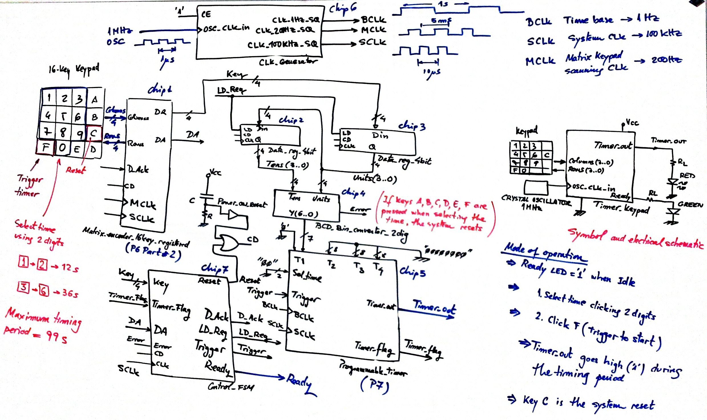 |
Fig. 2. Schematic (click to zoom). Discuss what section of the circuit is the datapath, and which wires are: status signals, control inputs, control outputs data inputs and data outputs. |
- Chip 6. Plan the CLK_generator.vhd. Explain how it works and the signals generated, adapting it to your board.
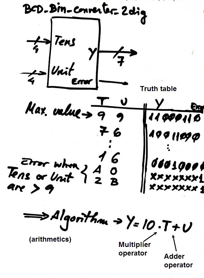
- Chip 4. Design the combinational circuit BCD_BIN_converter_2dig (symbol) used for translating the BCD keypad codes to a binary number, thus it can be understood by the programmable timer. In this application the maximum value that can be programmed is 99 s corresponding to the 7-bit radix-2 number "1100011".
Let us show you the power of VHDL synthesising algorithms in hardware. These are two proposed plans.
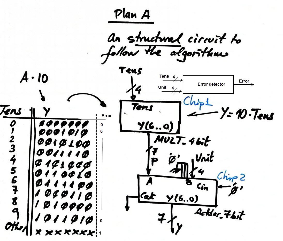
- Plan A is structural as it was learnt in P3.
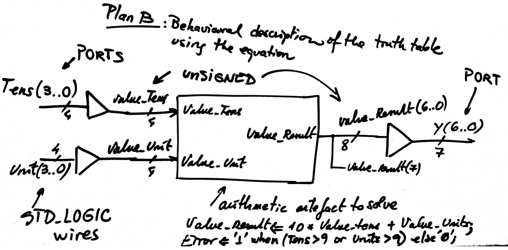
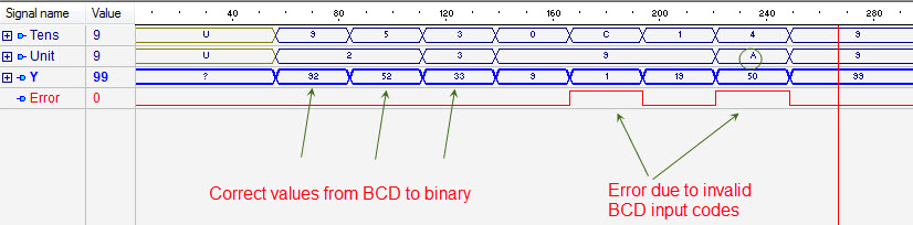
- Plan B is behavioural schematic. Write the code VHDL, inspect the RTL, the technology and test it functionally or at the gate-level using for example this test bench.
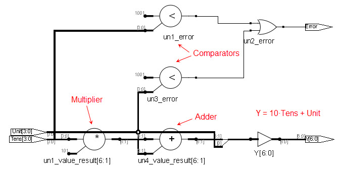 |
Fig. 4. RTL view of the plan B converter's equation. |
- Chip 1. Matrix_encoder_16key_registered from D2.15.
- Find VHDL code for the data registers.
- Discuss the state diagram for the Chip 7 Control_FSM.
- Mount the top circuit assembling all the components into a single project.
- While examining the RTL schematic, be aware of the number of registers (D_FF) used in the target chip and justify the value. Does it match with your initial estimation?
| Home Term 23/24-Q2 Contact Products Electronic devices and companies Software Books Magazines Instruments DEE Library EETAC DEEL |

|
|
| Web activa des de 09/2001, @ F. J. Robert, J. Jordana. Web editat amb Microsoft Expression Web 4. El contingut és un complement als materials d'estudi del curs Circuits i Sistemes Digitals disponibles al campus digital Atenea. Llicència:Reconeixement 4.0 Internacional de Creative Commons |