|
|
Bachelor's Degree in Telecommunications Systems and in Network Engineering |
|
|
|
|||||
Chapter 1 problems |
- D1.14 - |
9-bit parity generator, parity checker |
|||
|
|
|||||
1. Specifications
The project objective is to design a 8-bit data transmitter and receiver system with parity bit generator and checker. Fig. 1 shows the idea. The circuit relies on the component Parity_9bit type 74LS280. Transmission channel induced errors of 1-bit switch can be simulated using a XOR gate. If the data received is wrong and error flag is generated and the received byte is reset. Implement the system in VHDL using plan C2.
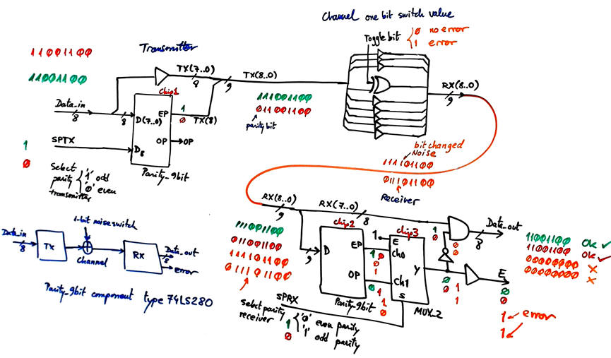 |
| Fig. 1. 8-bit parallel transmission system with addition parity bit. |
Draw an example of timing diagram to be used later as stimulus in the VHDL testbench when verifying the synthesised circuit. Consider Min_Pulse = 3.78 ms.
CPLD or FPGA target chip options:
Target option #1.: MAX II
Target option #2.: MAX 10
Target option #3.: Cyclone IV
This transmission system can be serialised in P7 and P8 using shift registers, as shown in the tutorial USART.
| Home Term 23/24-Q2 Contact Products Electronic devices and companies Software Books Magazines Instruments DEE Library EETAC DEEL |

|
|
| Web activa des de 09/2001, @ F. J. Robert, J. Jordana. Web editat amb Microsoft Expression Web 4. El contingut és un complement als materials d'estudi del curs Circuits i Sistemes Digitals disponibles al campus digital Atenea. Llicència:Reconeixement 4.0 Internacional de Creative Commons |