|
|
Bachelor's Degree in Telecommunications Systems and in Network Engineering |
|
|
|
|||||
Chapter 3 problems |
- B3.2 - |
BCD_7seg_decoder chip (μC - C) |
|||
|
|
|||||
1. Specifications
Design a BCD_7seg_decoder chip using a PIC18F4520.
The same project is proposed in D1.2 as a combinational circuit based on logic gates.
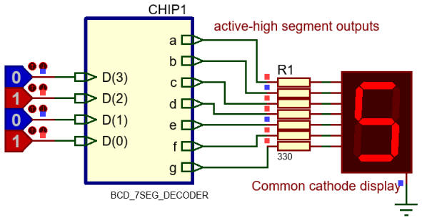 |
Fig.1. When operating, this decoder only deals with inputs from 0 to 9 ("0000" to "1001"). The remaining 6 combinations are of no interest. |
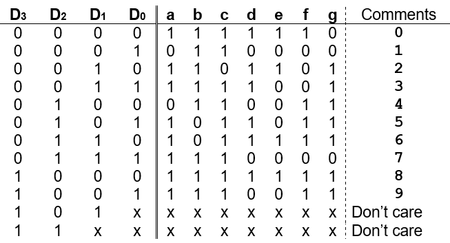 |
Fig.2. Truth table definition as an incomplete circuit. |
Some questions to organise the project:
Use the following pin connections:
D3 --> RA2; D2 --> RA3; D1 --> RA0; D0 --> RA1
a --> RB7; b --> RB6; c --> RC5; d --> RC4; e --> RD7; f --> RC1; g --> RC0
- List all the RAM variables involved in this design.
From a simiar tutorial in P9 or LAB9 where to copy and adapt to the project location folder:
- Draw an sketch of the hardware circuit and capture it in Proteus BCD_7seg_decoder.pdsprj
- Write the software source file BCD_7seg_decoder.c. Start an MPLABX - XC8 project targeted to the PIC18F4520 chip. Use our software organisation.
As we have decided, start compiling and testing one input or output at a time:
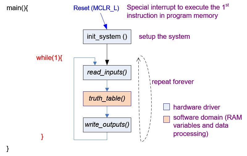
- Write the funcion init_system(). Start configuring only one input, compile and test. Describe using pictures and annotations how you are configuring registers.
- Write the funcion read_inputs(). Start reading only one input, compile and test. Describe using pictures and annotations how you are reading an input using bitwise C instructions.
- Write the funcion write_outputs(). Start writing only one output, compile and test. Describe using pictures and annotations how you are writing a RAM variable in the corresponding pin using bitwise C instructions.
- Translate the truth table to C code and complete truth_table().
- Check the full project and report.
| Home Term 24/25-Q1 Contact Products Electronic devices and companies Software Books Magazines Instruments DEE Library EETAC DEEL |

|
|
| Web activa des de 09/2001, @ F. J. Robert, J. Jordana. Web editat amb Microsoft Expression Web 4. El contingut és un complement als materials d'estudi del curs Circuits i Sistemes Digitals disponibles al campus digital Atenea. Llicència:Reconeixement 4.0 Internacional de Creative Commons |