|
|
Bachelor's Degree in Telecommunications Systems and in Network Engineering |
|
|
|
||
|
|
4-bit serial multiplier (add & shift algorithm) |
|
|
|
||
Dedicated processor (datapath + control unit)
1. Specifications
Note: review, update: This project follows former CSD naming conventions and styles and is not yet updated. It has to be rewritten contextualising this application again as a dedicated processor. Comparison of a hardware combinational multiplier and this serial multiplier.
Cooperative groups will have to specify, plan, develop, simulate, implement and prototype a complex application such as serial multiplier.
-
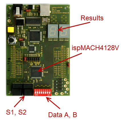
2- BCD digits to display the result (Board HWD-LC4128V, Lattice CPLD chip).
-
A set of 8 switches to input A and B operands, or alternatively a matrix keyboard.
-
20 kHz clock synchronous system.
-
Pushbuttons to start operation, visualise results, and a LED for signalling the end of operation.
-
Serial add-and-shift algorithm.
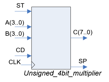
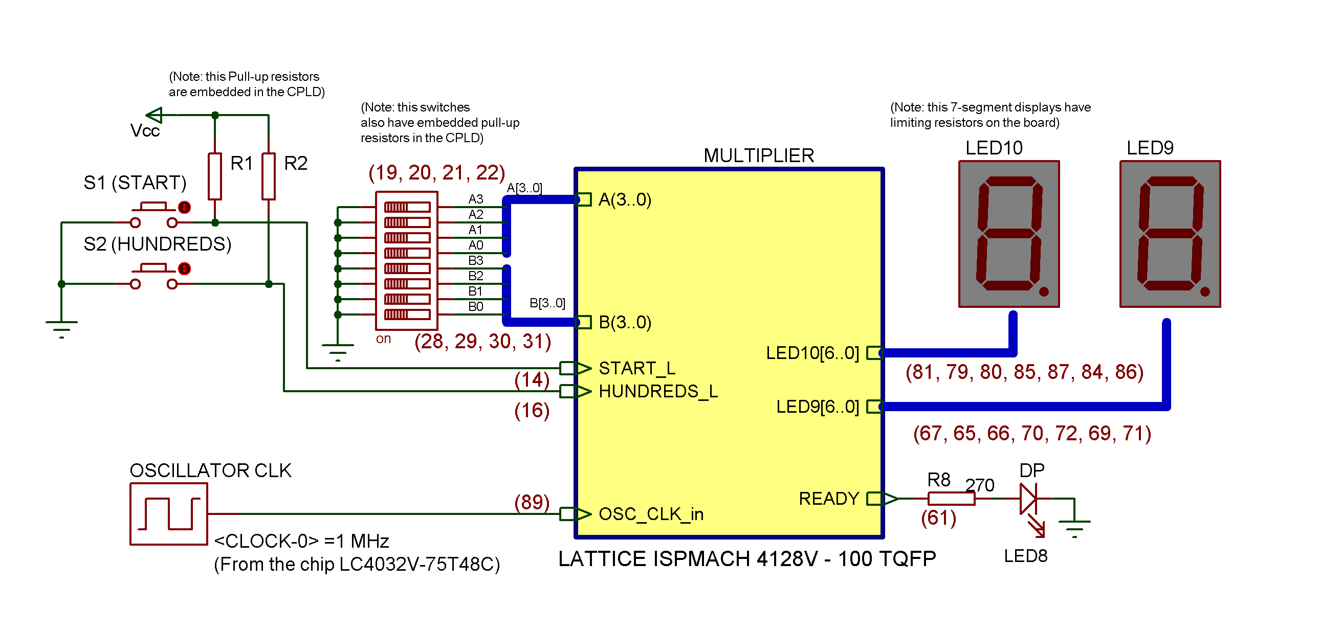
Fig. 1 shows the symbol, the top level scheamatic to adapt the design to HWD-LC4128V prototyping board and the pin assigment for inputs and outputs (switches, buttons, LEDs and 7-segment digits). This is the visio of the symbol.
Class notes (pdf1) (pdf2) (pdf3) (pdf4) (pdf5) (pdf6) on problem discussion.
 |
|
  |
|
|
2. Plan C2 based on a dedicated processor
Devising a plan:
- The project much be finished before the due date.
- As discussed in previous section, the idea is organise the problem top-down, and then go back bottom-up.
- Each cooperative group will be in charge of the design of a multipliers component.
- The VHDL programming style for the components will be exemplified through the design of the data register.
- Some important blocks, like the multipliers control unit will be solved by every student individually.
- Fig 2: The top architecture [G7].
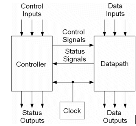 |
| Fig. 2. Architecture of a dedicated processor. |
3. Development
Top architecture and components.
 |
| Fig. 3. Complete planning using a dedicated processor architecture. |
 |
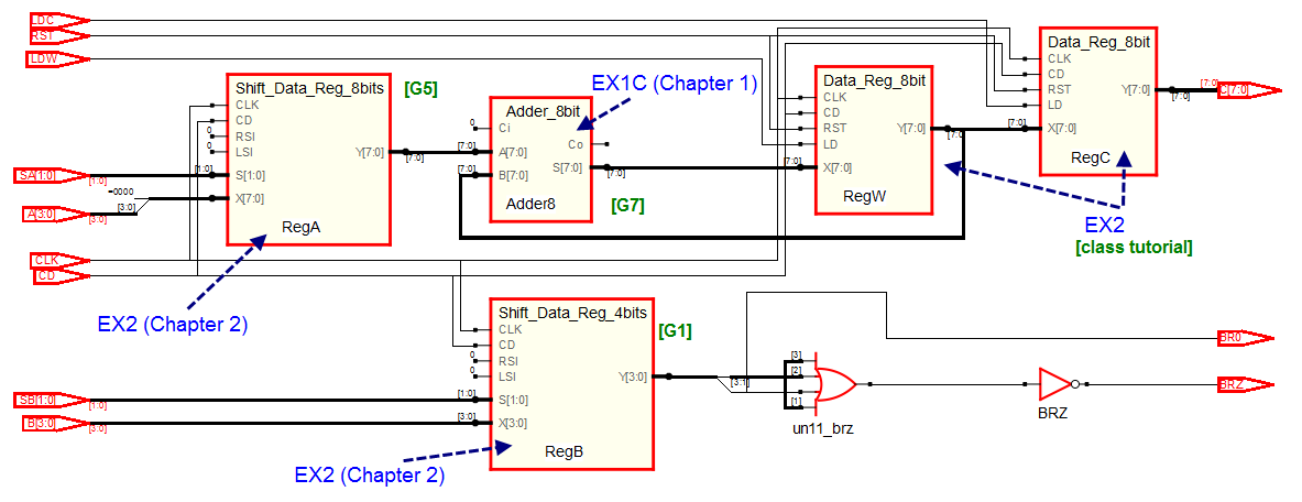
| Fig 4: Internal architecture of the unsigned multiplier as a dedicated processor. |
 |
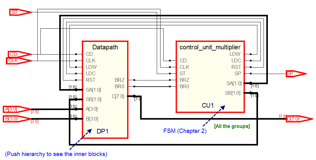
| Fig 5: Structural RTL level architecture of the datapath and control unit. |
Each group designs their component using the typical PLD design flow (symbol, specifications (truth table for a CC, state diagram or/and timing diagram for a SS), ActiveHDL project, functional simulation using a ispLEVER-generated test bench, RTL schematic, gate-level simulation of the synthesised circuit, analysis of used resource used, and reporting.
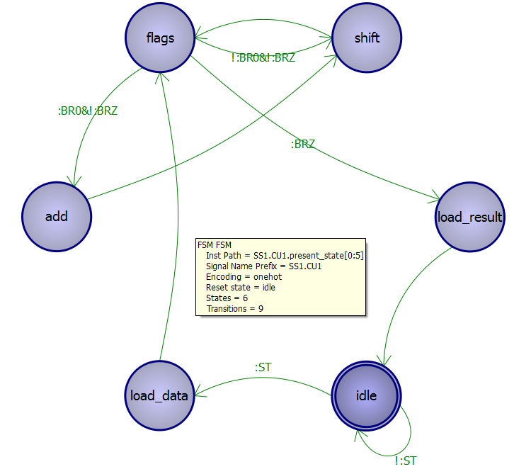 |
Fig. 6. State diagram of the FSM control unit. |
All the VHDL files.
| Number of VHDL files involved | Block to be designed and some remarks | Entity name (VHD) / top design | Components (hierarchy level 1) | Components (hierarchy level 2) | Components (hierarchy level 3) |
| 21 | Multiplier (the top entity) | multiplier.vhd | (This file is the structure of the top entity, as shown above in Fig 1) | ||
| 8 | The 4x4
unsigned serial multiplier |
unsigned_4bit_multiplier.vhd |
Datapath.vhd |
Data_Reg_8bit.vhd
Shift_Data_Reg_8bits.vhd Shift_Data_Reg_4bits.vhd |
|
| Adder_8bit.vhd | One_bit_adder.vhd | ||||
| control_unit_multiplier.vhd | |||||
| 3 | 5 s timer. This is
a complex digital system in itself: a datapath, in this case
a counter, controlled by a FSM |
timer.vhd |
counter.vhd control_unit_timer.vhd |
||
| 1 | 4MUX4 (Chapter 1) | Quad_MUX4.vhd | |||
| 2 | Code converter from
binary to BCD (Units, tens and Hundreds) (Chapter 1, see a truth table and a block diagram for the 74185 chip) |
Bin_BCD_converter_8bit.vhd | Bin_BCD_type74185.vhd | ||
| 1 | Binary to 7 segment decoder with "H" symbol. | BCD_7seg.vhd | |||
| 5 | Clock divider | OSC_FREQ_DIV.vhd |
Freq_Div_100.vhd Freq_Div_50.vhd Freq_Div_2.vhd T_Flip_Flop.vhd |
||
4. Test (functional)
Design the Active-HDL test bench for the top Multiplier project.
Functional simulation.
5. Test (gate-level)
Gate-level simulation.
6. Prototyping
Demonstrate how the board works for real as a laboratory prototype.
Add other features, link the project with other or learn on how th implement multipliers using different algorithms
7. Report
Example of report for this project (Author: Angélica Rodríguez Sánchez).
Other questions: How to multiply 8x8 bit numbers using an 4x4 multiplier?
| Home Term 24/25-Q2 Contact Products Electronic devices and companies Software Books Magazines Instruments DEE Library EETAC DEEL |

|
|
| Web activa des de 09/2001, @ F. J. Robert, Web editat amb Microsoft Expression Web 4. El contingut és un complement als materials d'estudi del curs Circuits i Sistemes Digitals disponibles al campus digital Atenea. Llicència:Reconeixement 4.0 Internacional de Creative Commons |