|
|
||
|
|
CLK generator circuit |
|
|
|
||
1. Specifications
In this application are required up to four square synchronous CLK signals at 100 kHz, 1.6 kHz, 20 Hz and 1 Hz. We will consider a 50 MHz input OSC_CLK_in.
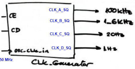 |
Fig. 1. Symbol of the CLK_generator |
2. Planning
As discussed in L8.2, we will use the generalised plan C2 schematic that works chaining frequency dividers (freq_div_Mod, invented using plan Y) and T_FF for squaring the pulsed waveforms (and also an extra division by 2).
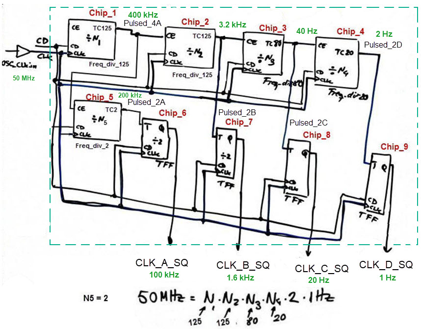 |
| Fig. 2. CLK_Generator architecture based on frequency dividers and T_FF memory cells. |
Fig. 3 shows a picture of the 50 MHz quartz crystal populating the Terasic DE0.
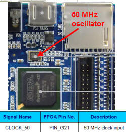 |
Fig. 3. Intel DE0 board 50 MHz oscillator from which we will derive the synchronous squared CLK signals of: 100 kHz, 1.6 kHz, 20 Hz, and 1 Hz required in this project. Many other prototyping board contain a similar quartz crystal. |
Another board like DE10-Lite has two identical 50 MHz CLK signals available for the FPGA at pins P11 and N14 from its own CLK generator: a specialised chip CDCE937.
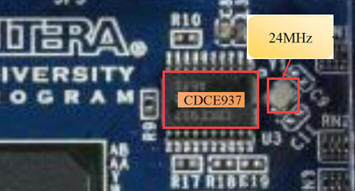 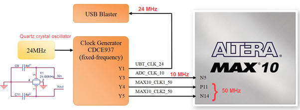 |
Fig. 4. Intel DE10-Lite board CLK circuit derived from a 24.00 MHz quartz crystal. |
Project location:
C:\CSD\P8\CLK_Generator\(files)
3. Development
Translating into VHDL the architecture in Fig. 2: CLK_Generator.vhd. This are its internal components: freq_div_125.vhd, freq_div_2.vhd, freq_div_20.vhd, freq_div_80.vhd, and the T_FF.vhd file is fetched from its T_FF.
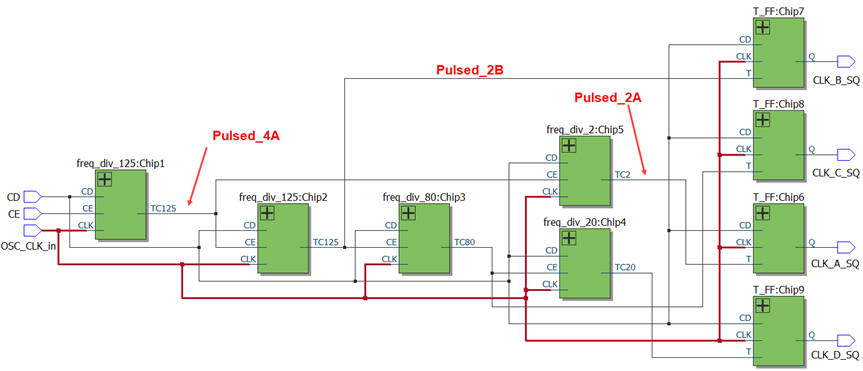
Picking up the FPGA MAX10 10M50DAF484C7G available in DE10-Lite board, we synthesise the RTL circuit represented in Fig. 5.
 |
|
Fig 5. CLK_Generator RTL schematic. We can check that this application requires 31 D_FF. |
 |
|
Fig 6. Technology view of this synchronous design. |
4. Test (functional)
Generate a skeleton of the testbench for simulating the CLK_Generator circuit. This is a valid testbench file CLK_Generator_tb.vhd from which to copy stimulus and CLK processes. CLK_Period = 20 ns.
Hint: in case of simulating the CLK_Generator as a component, because it is about counting tens of millions of pulses, there is a way to speed up the simulation tricking the frequency dividers while keeping the number of registers used and everything else, as shown in Fig.6. The output waveforms will be of different frequencies, but they will be synchronous and identical as in the real CLK_Generator which has to be configured in the real hardware.
 |
| Fig. 6. Modification in the VHDL code to speed up the simulations of the CLK_Generator component. |
Zooming through the time scale and using cursors we can measure waveform periods and frequencies.
  |
|
Fig 7. Simulation results representing CLK waveforms pictured at different time scales. |


