|
|
Bachelor's Degree in Telecommunications Systems and in Network Engineering |
|
P6: Finite state machines (FSM) |
| Resources in lectures and labs: | L6.1, Lab6, L6.2 | Project | objectives |
Highlighted project: 16-key matrix keypad encoder
| 1. Specifications | Planning | Developing | Test functional | Test gate-level | Report | Prototype |
Design a 16-key keyboard scanner similar to MM74C922 chip that can be taken as a model to discuss basic features. Apply our FSM proceeding. Fig 1 shows the symbol. The output Data(3..0) vector represents the hexadecimal code of the key pressed rec.
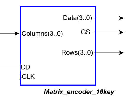 |
Fig 1. Symbol (Visio) of the Matrix_encoder_16key to be designed using a FSM architecture. This circuit can be compared to the combinational equivalent Enc_16_4 studied in P2. |
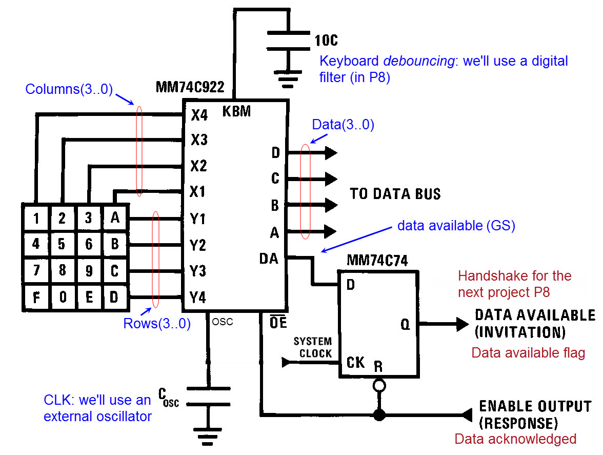
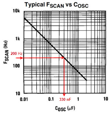
Some theory on how a matrix keypad operates: this Proteus simulation is a 16-key matrix keyboard component. As recommended in the classic chip MM74C922 (see the Fig. 2), a CLK frequency 200 Hz may be a convenient for scanning keys (use a COSC = 330 nF). This is yet another Proteus simulation of the complete MM74C922 chip running as a 16-key matrix encoder.
 |
 |
| Fig 2. Connecting the MM74C922 to a keypad as described in the datasheet. Details on how the scanning frequency can be fixed for this chip when using its internal oscillator. |
|
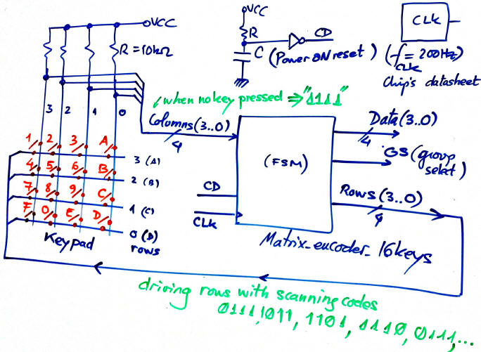
Therefore, the circuit to invent has to be similar to Fig. 3. Power-ON reset can be used to initialise the FSM after connecting the power supply.
 |
|
| Fig 3. Circuit to scan rows and read columns. | |
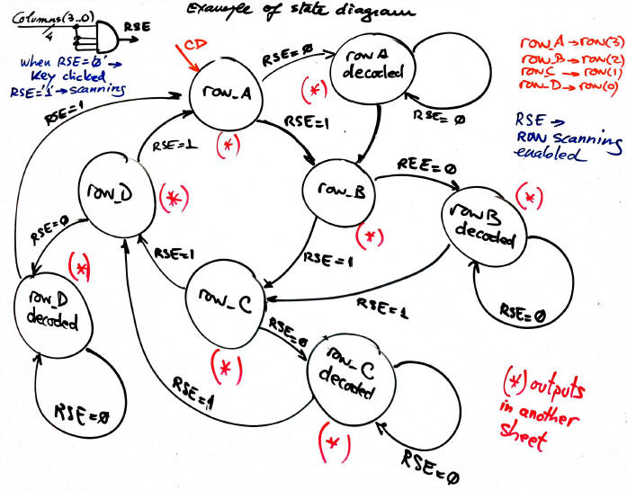
Propose a state diagram to figure out how the matrix scanner works on the basis of a FSM. Fig. 4 shows an example considering the signal Row Scanning Enabled (RSE) derived from Columns(3..0) which is '1' when no keys are pressed. In each state all the output values must be set, and for clarity reasons it is indicated as (*) to be represented in another sheet op paper. Discuss which may be the output values in each state.
 |
|
Fig 4. Architecture of the 16-key matrix keyboard encoder FSM and some other planning ideas (click to zoom). |
Draw an example of a timing diagram as in Fig. 5 because precisely in this problem is not so easy to comprehend which kind of signals are intervening in the system and when. Draw it analysing the state diagram for better understanding. Watch the rec. as well because this time, a video sequence is much better than a final photograph.
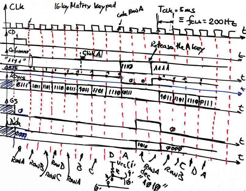 |
| Fig 5. Discuss an example of a timing diagram imagining the Columns(3..0) vector values that will be read from the keypad. How the circuit is initialised? |
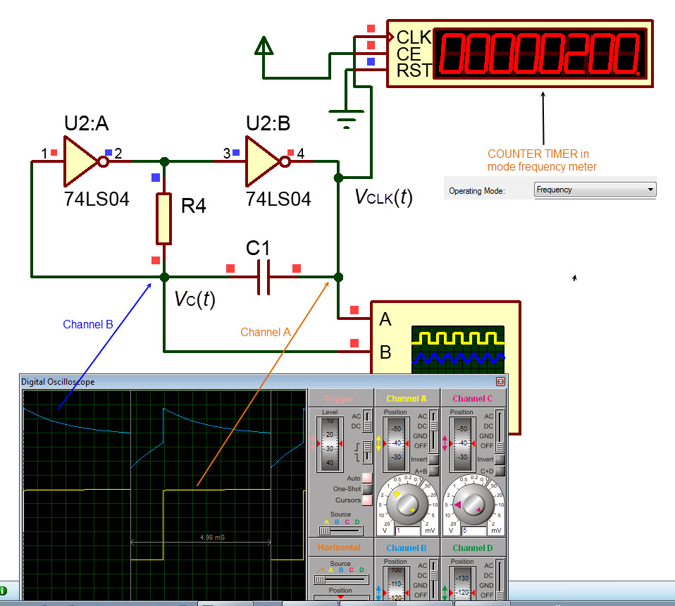
Optional. Additional task: replace the ideal CLK block in the Proteus schematic, by an oscillator circuit (CLK) based on NOT gates (in LS-TTL technology) and resistors and capacitors adjusting the CLK frequency OSC_FREQ to the given value, for instance 200 Hz (Fig. 2). You have to deduce the formula of the frequency of oscillation as a function of the external components OSC_FREQ = f(R, C). See this schematic. Or instead, use the integrated circuit 555 obtain an oscillator (astable, multivibrator).
Optional. What happens when clicking several keys at the same time? (when is at the same time in this context?) Is it possible to think on priority-high encoding as we did for the 74LS148 chip when clicking several keys simultaneously? Studying this problem may be an enhancement for a second design phase. And at this point, there is much more to learn on key rollover, jamming and ghosting to get a good introduction to modern keyboard techniques.
Other design tutorials and assignments.
| Specifications | 2. Planning | Developing | Test functional | Test gate-level | Report | Prototype |
Devising a strategy to solve the problem. This is the engineer's job and the most difficult task. Generally, many teams intervene planning top-down strategies to conceive how modules and components can be assembled and interconnected. As you have seen in the many projects solved hitherto, our plan must be in the end a detailed "camera-ready" schematic for an effortless VHDL translation when starting development.
Let's implement the FSM capable of solving the state diagram above. Let's us discuss the adaptation of the FSM to our problem as shown in Fig. 6.
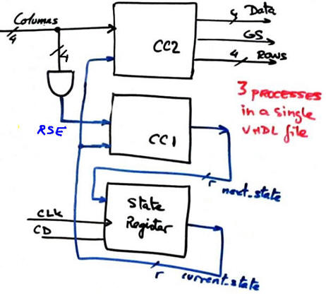 |
Fig 6. This is the adaptation of the general FSM architecture to the problem. We will keep this hierarchical circuit in the same VHDL file (plan C1); each block will be written as a PROCESS (instead of components as it is in plan C2) |
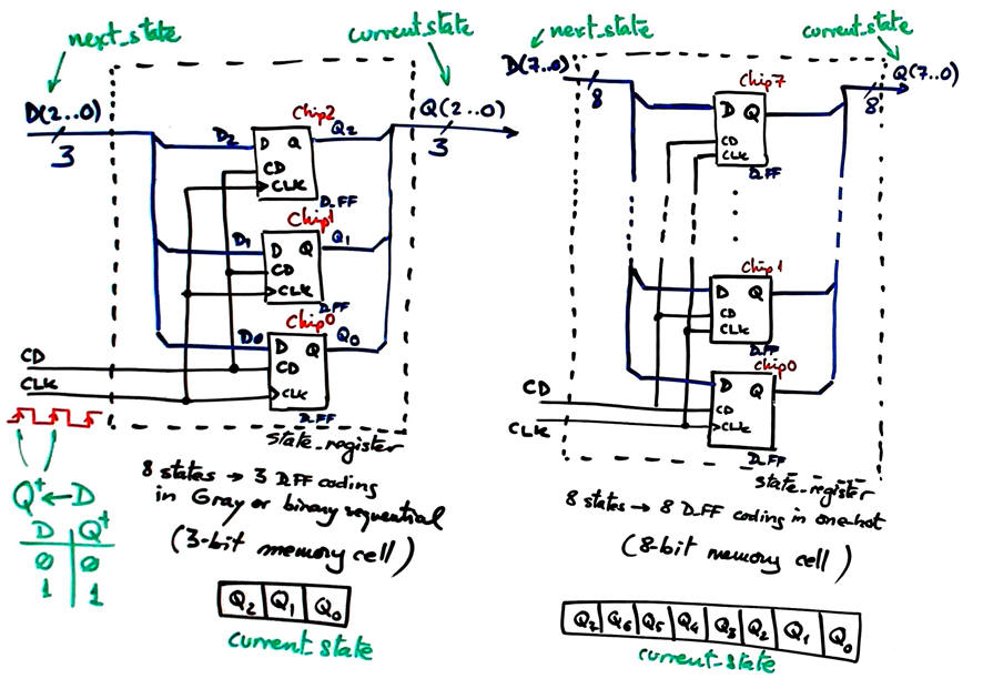
How many D_FF (1-bit synchronous data registers) will include the state register memory to encode the FSM states when coding in one-hot, binary radix-2 (sequential) or Gray? Draw a synchronous state register for this application.
 |
|
| Fig 7. Draw the state register for this application based on D_FF. For instance, when coding in binary sequential only 3 D_FF are required, but 8 D_FF when coding states in one-hot. In this way the system has a memory cell to "remember" its current internal state. |
|
Let us write the truth table for the CC2 circuit as below in Fig. 8.
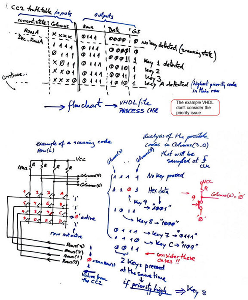 |
Fig 8. The CC2 truth table discussion. It is about determining which outputs are required in each state. |
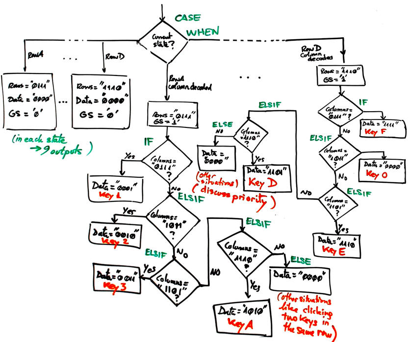
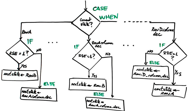
Continue with the translation of the CC2 truth table using a behavioural interpretation based on flowcharts or ASM (algorithmic state machine) diagrams. This plan B is referred as the strategy number 8 for designing logic circuits.
 |
|
| Fig 9. Translating CC2 truth table into a flowchart. |
|
-
Let us write the truth table for the CC1 circuit as in Fig. 10.
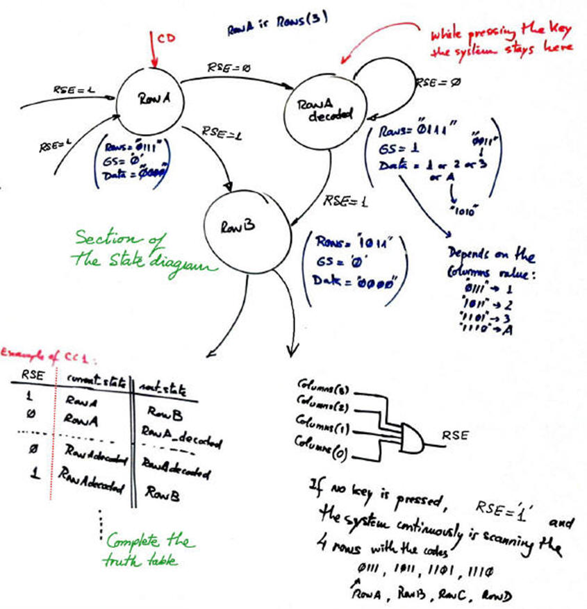 |
| Fig 10. Example of CC1 discussion. All the state transitions must be considered in the table. |
Continue with the translation of the CC1 truth table using a behavioural interpretation based on flowcharts or ASM (algorithmic state machine) diagrams.
 |
|
| Fig 11. Discuss the translation of the CC1 truth table into a flowchart. |
|
Project location:
C:\CSD\P6\Matrix_encoder_16key\(files)
| Specifications | Planning | 3. Developing | Test functional | Test gate-level | Report | Prototype |
Carrying out the plan usually is the job of an engineer or better a technician when planning phase is complete. In the same way that an architect is not required every day in the construction site.
Here we have to write the previous schematics, truth tables and flowcharts in a single VHDL source file like this Matrix_encoder_16key.vhd based on our CSD style. Start a new project using an EDA tool and synthesise a circuit for a specific target CPLD or FPGA target chip.
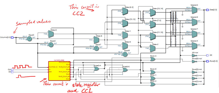
In our project, the RTL view must show the main details of the FSM. Print and comment the schematic indicating the main components CC1, CC2 and the state register. Be aware that this schematic depends on the EDA tool where each one has its own style for representing the ideal circuits interpreted from VHDL files.
 |
|
Fig 12. Example of an RTL schematic (using Quartus Prime). |
Fig. 13 is an example of state diagram as drawn by Synplify Pro Lattice edition that can be inspected from the RTL view. Try other tools such as Intel Quartus Prime.
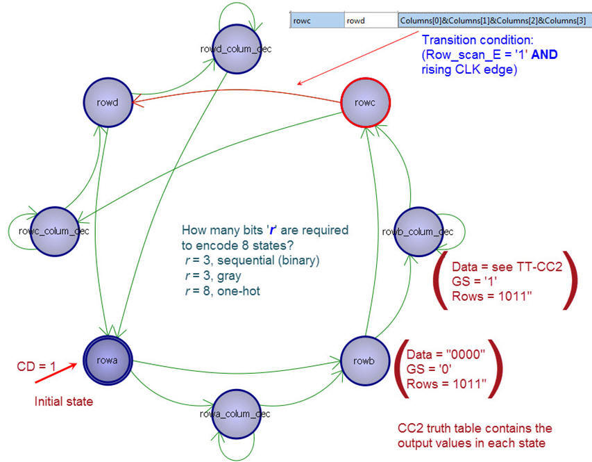 |
Fig 13. Example of state diagram represented automatically by the EDA tool. |
And below in Fig. 14 there is the default encoding (onehot), which means that 8 D_FF are required.
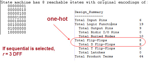 |
Fig 14. Encoding states in this application. |
Below in Fig. 15 is the technology view of the circuit being synthesised, which give you an idea of the design complexity and resources (instances) used. Count and check that the number of registers D_FF is what is expected accordingly to the chosen state encoding (binary sequential, Gray, one-hot).
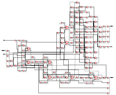 |
Fig 15. Example of a technology view (click to zoom). |
Check the resources used in the project summary: chip pins, LUT's, slices, registers D_FF, etc.
| Specifications | Planning | Developing | 4. Test functional | Test gate-level | Report | Prototype |
Examining test results, engineers must look back to see whether the device comply with the specifications; and forward to see which modifications may achieve better performance. Engineers must be able to organise test procedures to verify that the system works as expected before the next prototyping stage in the laboratory.
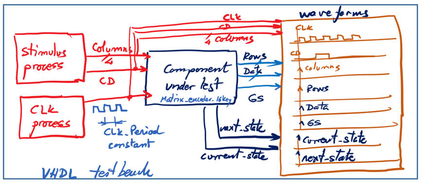
In Fig. 16 is represented the VHDL test bench fixture for testing this application. A separated process will run continuously to generate the periodic signal CLK.
 |
||
Fig 16. Testbench schematic. It is generated automatically as a template from the EDA tool project navigator and then the user can add the stimulus from the timing diagram in Fig. 4 and the CLK process. |
||
Generate from Quartus Prime the testbench fixture skeleton in Fig. 16. Rename it and move it to the project folder.
Copy from this example file matrix_encoder_16key_tb.vhd only the stimulus activity described in the two processes and also the constant CLK_Period.
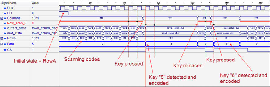
Start and run a functional simulation project using ModelSim to verify that the device operates like expected in the initial timing diagram sketch in Fig. 4. Some results are represented in Fig. 17. Going down one level in the hierarchy to pinpoint the instance i1, drag to the wave diagram the internal signals current_state and next_state.
Modify the stimulus process to include other inputs. The circuit must work correctly for the 16 keys.
 |
|
Fig 17. Functional simulation with annotations and discussion to determine whether the circuit works as expected. |
|
| Specifications | Planning | Developing | Test functional | 5. Test gate-level | Report | Prototype |
Perform a gate level simulation to measure the propagation time from CLK to output (tCO) for a given technology. For instance, Lattice ispMACH4128V CPLD, Xilinx Spartan-3E XC3S500E-FG320 or Intel MAX II EPM2210F324C3. Select a convenient CLK rising edge transition and measure how long does it take to have stable outputs.
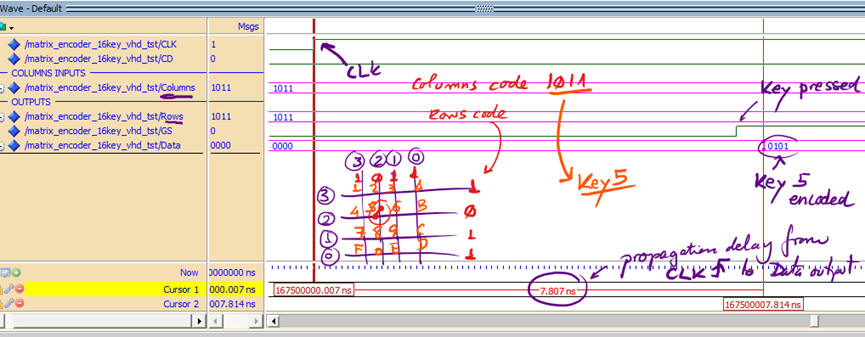 |
| Fig 18. Example of gate level simulations at a given CLK transition. |
Using the timer analyser tool, we can determine the worst-case scenario, thus, determine the maximum processing speed of this circuit. A question equivalent to asking how fast can be scanning and encoding the keypad (in case of not having parasitic effects and key bouncing problems)?
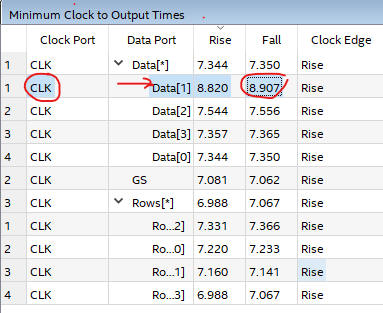 |
Fig 19. The timing analyser tool can be used to measure
the maximum speed of the system CLK: |
Here, if we like to go further, we can take advantage of the easiness in using EDA tools. For instance, we can compare circuit realisations and answer questions such:
1) What circuit is faster, the one using onehot or the one using a sequential-binary encoding (CC2 combinational blocks are different)?
2) What circuit uses more chip resources? Such answer can be deduced inspecting project summaries.
3) What technology FPGA, CPLD is faster solving the project?
| Specifications | Planning | Developing | Test functional | Test gate-level | 6. Report | Prototype |
By now, you know very well how document your project and what is assessed. Project report: sheets of paper, scanned figures, file listings, notes or any other resources. Follow this rubric for writing reports.
Therefore, try to self-assess your project using the rubric discussed in class. It's interesting to look back and annotate remarkable questions that were raised while working on the projects (thanks to students deep engagement and discussion), that in the end can be used to generate a higher quality device (advanced project):
- Why the system gets stuck when the
matrix CLK frequency is too high?
- What can be done to prevent the hanging of the system and how it can
recover automatically to a known state?
- Which is the advantage of using debouncing filters in each column?
- What can be done to design a system with all the outputs fully
synchronised?
- What can be done to read/sample the columns on the rising edge of the
CLK, so that they are going to be kept saved until the next rising
edge?
| Specifications | Planning | Developing | Test functional | Test gate-level | Report | 7. Prototype |
Use training boards and perform laboratory measurements to verify how the circuit works.
It is interesting in order to see how the circuit works, to use some extra LED to visualise signals and data, which implies building a top schematic containing for instance a HEX_7SEG_DECODER to represent the 16 hexadecimal symbols. This is the top schematic to be implemented in the HWDLC4128V board (schematic) populated with a ispMACH4128V CPLD from Lattice Semiconductor. And this is the RTL view interpreted by Synplify Pro synthesiser tool.
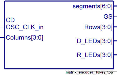 |
Fig 20. The top schematic symbol that includes some extra ports for debugging purposes generated by the ispLEVER Classic. This is the complete zipped project where you can examine the top VHDL file. |
Once the development board has been chosen, we have to assign PLD pins to inputs and outputs. This task is conveniently done using the spreadsheet "Constrain Editor", as represented in Fig. 21.
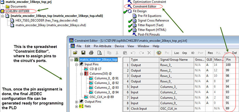 |
Fig 21. Using the Constrain Editor for pin assignments available through the ispLEVER Classic project navigator. |
So that the final configuration file *.JED can be downloaded into the chip. This task is performed as shown in Fig. 22, by a chip programmer tool like the ispVM System from Lattice Semiconductor.
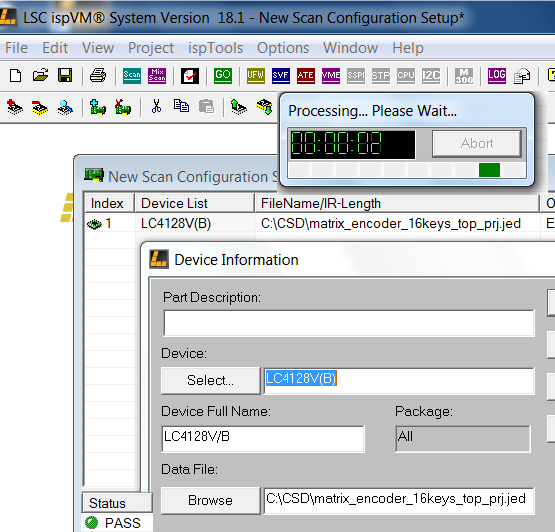 |
Fig 22. This is the ispVM System tool to be used for chip programing. The development board is connected to the computer using a simple USB interface and the tool scans the hardware to detect which is the chip populating the board. Clicking GO the PLD is programmed in a few seconds. For sPLD or CPLD technologies, the programming of the macrocells is permanent and only can be erased reprogramming he chip another time with the same or a different configuration. For FPGA technologies, the programming of the LUT (look-up tables) is volatile, and the RAM is erased once unplugged from the power supply. Thus, usually boards contain a supportive EEPROM memory to save the FPGA configuration rewriting the RAM every time the board is powered.
|
Finally, we can experiment with the prototype represented in Fig. 23 in order to see whether all the specifications has been met, as shown in this rec. Many times the real circuit, as it was in the simulations, does not fully work, and so, a design loop (Visio) must be started again to modify schematics, rewrite VHDL code and synthesise and program again.
 |
Fig 23. This is a picture of the scanning keyboard running on a Lattice ispMACH4128V CPLD target chip (click to zoom). |
| Home Term 24/25-Q1 Contact Products Electronic devices and companies Software Books Magazines Instruments DEE Library EETAC DEEL |

|
|
| Web activa des de 09/2001, @ F. J. Robert, J. Jordana. Web editat amb Microsoft Expression Web 4. El contingut és un complement als materials d'estudi del curs Circuits i Sistemes Digitals disponibles al campus digital Atenea. Llicència:Reconeixement 4.0 Internacional de Creative Commons |