|
|
Bachelor's Degree in Telecommunications Systems and in Network Engineering |
|
| Analysis and design tutorials | Analysis and design assignments | Prototypes | Exam 1 | Exam 2 | Questions and assessment |
CSD EXA1: midterm exam examples and solution ideas |
1617Q2
Problem 1
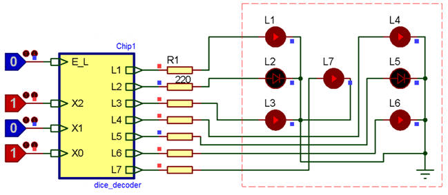
The entity represented in Fig. 1a is an electronic dice decoder, a combinational block for adapting the binary numbers from 1 to 6 to a 7-LED display that has the typical layout shown in Fig. 1b. Codes “000” and “111” don’t care.
 a) a)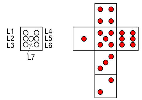 b) b) |
Fig. 1. Circuit for driving an electronic dice. |
1. Deduce the decoder truth table of all the outputs Li = f (E_L, X2, X1, X0).
2. Describe the algebraic expression of L3 as a product of maxterms.
3. Describe the algebraic expression of L1 as a sum of minterms.
4. Express the output L6 using only NAND.
5. Implement the output L7 using the method of multiplexers (MoM) and a MUX_4 component.
6. Draw a behavioural flow chart (plan B) for the dice_decoder and translate it to VHDL.
7. Using the method of decoders (MoD), draw a schematic for the dice_decoder and write it in VHDL. How many files are required?
8. If the following table in Fig. 2 represents the output from Minilog when inputting the dice_decoder truth table and simplifying by PoS, write down the equations for the outputs L4 and L6.
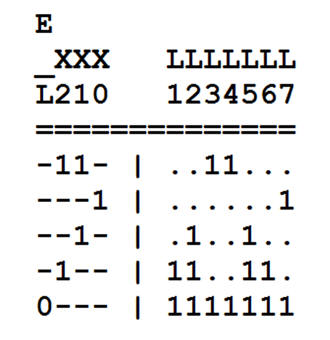 |
Fig. 2. Output table format from Minilog.exe. |
9. Solve the arithmetic operations in Fig. 3 using 8-bit 2C (two’s complement) number representation. Indicate when there is an overflow situation (OV flag). Which is the valid range of the operands and operations?
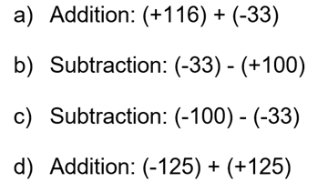 |
Fig. 3. Add and subtract in 8-bit 2C convention. |
10. Propose a circuit structure able to perform the 8-bit 2C
operations in 9).
Solution ideas
Most of the answers can be found in lectures from P1 to P4. This is the Proteus "dice_decoder.pdsprj" file, the "dice_decoder.tbl" in Minilog and the "dice_decoder.min" results when simplifying by PoS.
Problem 2
The entity represented in Fig. 4 is a code converter from BCD to Johnson. Only ten of the sixteen input combinations are possible, thus the other terms are don’t care ('x' or '-'). Complete the truth table in Fig. 4 and solve the questions below.
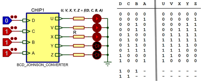 |
Fig. 4. The circuit for a BCD to Johnson ring code translator and its truth table. |
1. Describe the algebraic expression of V as a product of maxterms and U as a sum of minterms.
2. From the table in Fig. 5, express Z as a sum of products (SoP), and draw the logic circuit using only 2-input NOR gates.
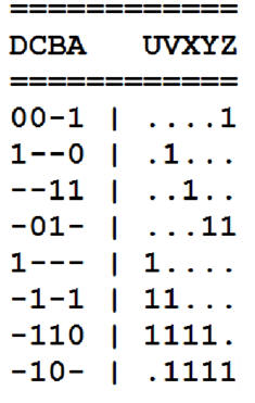 |
Fig. 5. Output table format from Minilog.exe in SoP. |
3. Build the circuit for the Y using the method of multiplexers and a MUX_8.
4. Build the complete circuit using the method of decoders.
5. Build the circuit using VHDL and a behavioural description of the truth table (plan B).
6. In Fig. 1, calculate the value of R for VCC = 5 V, technology LSTTL, and the LED current must be set to 2.5 mA.
7. If one gate of the circuit in 2) has a propagation delay of 3.3 ns, infer and discuss the circuit speed (millions of operations per second).
Solution ideas
Most of the answers can be found in lectures from P1 to P4.
The truth table "BCD_Johnson_converter.tbl" and the symbol "BCD_Johnson_converter.pdsprj" in Proteus that can be simulated attaching this "BCD_Johnson_converter.jed" to the AM22V10 sPLD.
This is the VHDL "BCD_Johnson_converter.vhd" file using plan B (question 5), and this is the ispLEVER Classic report "BCD_Johnson_converter.rpt" where you see the pin connections after synthesising the circuit.
| Home Term 26/27-Q1 Contact Products Electronic devices and companies Software Books Magazines Instruments DEE Library EETAC DEEL |

|
|
| Web activa des de 09/2001, @ F. J. Robert, Web editat amb Microsoft Expression Web 4. El contingut és un complement als materials d'estudi del curs Circuits i Sistemes Digitals disponibles al campus digital Atenea. Llicència:Reconeixement 4.0 Internacional de Creative Commons |