|
|
Bachelor's Degree in Telecommunications Systems and in Network Engineering |
|
|
|
|||
|
|
Circuits based on logic gates |
||
|
|
|||
Deduce Circuit_Q truth table using method I (Boole's algebra). Check results analysing the same Circuit_Q using method II based on Proteus simulations.
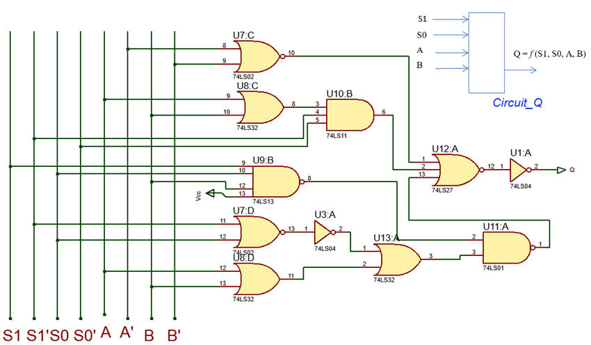 |
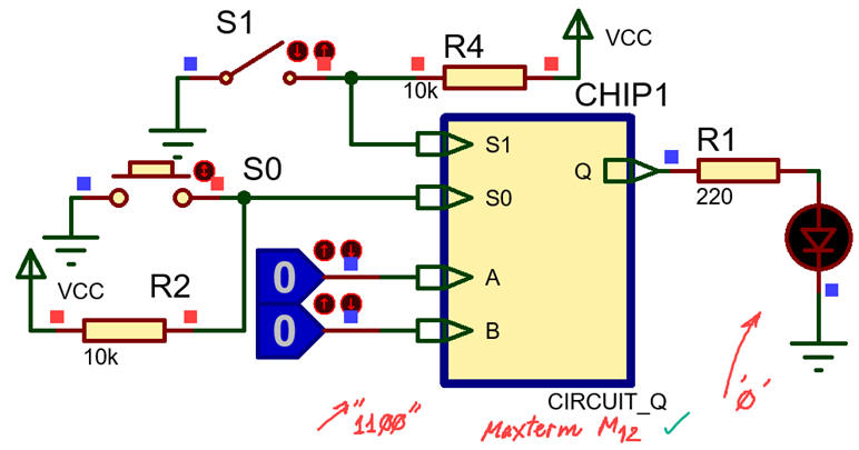
| Fig. 1. Circuit_Q based on logic gates. |
2. Planning the analysis
Analysing Circuit_Q means deducing how it works for every input binary combination represented by its truth table. Fig. 2 shows methods I and method II on how to do it.
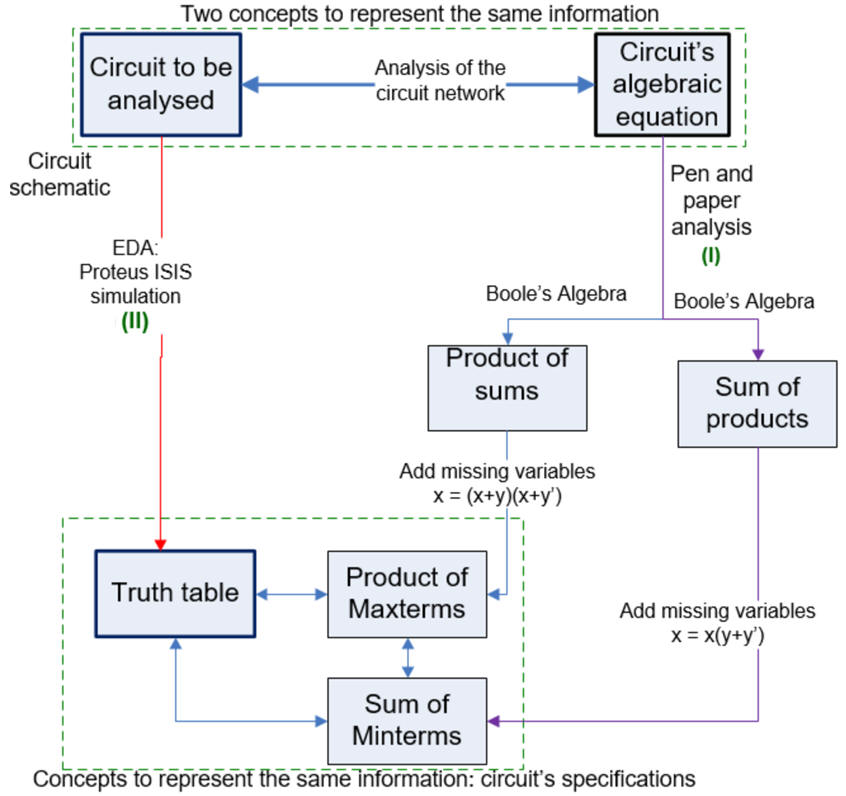 |
| Fig. 2. Concept map for solving Circuit_Q. |
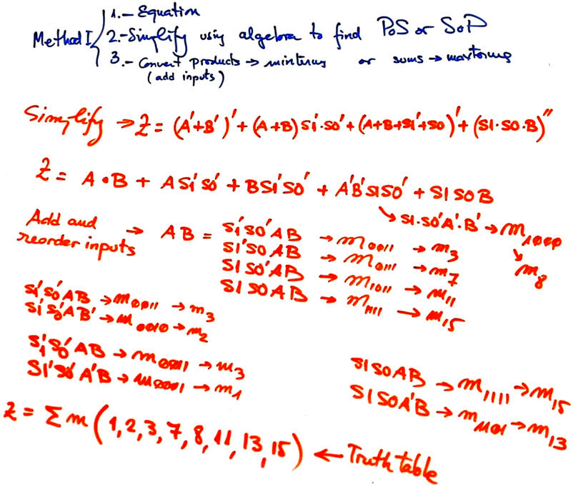
1. To proceed with method I deduce the circuit's equation and apply Boole's algebra to get firstly the SoP or the PoS and secondly, the sum of minterms or product of maxterms, which are conceptually the truth table itself.
2. To test the truth table using method II capture the circuit in Proteus and run simulations.
3. Developing the analysis project
Analysis. Each analysis will be developed using the necessary tools. For instance:
Method I: apply Boolean algebra to deduce the truth table and its minterms or maxterms.
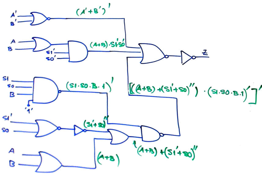 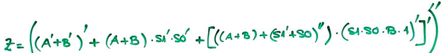 |
| Fig. 3. Circuit's algebraic equation. |
From the initial circuit equation in Fig. 3 and the simplification process using Boole's algebra, we deduce the circuit's truth table in Fig. 4.
 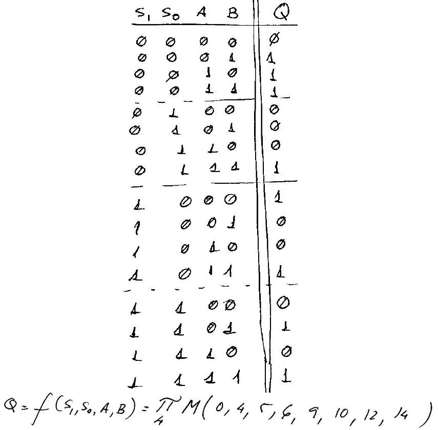 |
| Fig. 4. Circuit_Q truth table. |
4. Testing and validating analysis results
Method II: Draw Circuit_Q.pdsprj in Proteus using 74LS technology and run all input stimulus.
 |
| Fig. 5. Simulating Circuit_Q in Proteus. |
This is yet another way to verify Circuit_Q using method IV WolframAlpha equation.
5. Reporting the analysis
Using pictures, diagrams, sketches, handwriting discussions, etc.
| Home Term 26/27-Q1 Contact Products Electronic devices and companies Software Books Magazines Instruments DEE Library EETAC DEEL |

|
|
| Web activa des de 09/2001, @ F. J. Robert, Web editat amb Microsoft Expression Web 4. El contingut és un complement als materials d'estudi del curs Circuits i Sistemes Digitals disponibles al campus digital Atenea. Llicència:Reconeixement 4.0 Internacional de Creative Commons |