|
|
Bachelor's Degree in Telecommunications Systems and in Network Engineering. Bachelor's Degree in Aerospace Systems Engineering |
|
|
Power lamp PWM control using FPGA and VHDL tools |
| 1. Specifications | Planning | Developing | Test functional | Test gate-level | Report | Prototype |
This is the full project page for the dimmer's Option #B1: hardware design. Let us use the DE10_Lite FPGA board to provide a digital control of the lamp, as if this project were the CSD D2.5 version V2. The architecture will mimic the PIC PWM peripheral design.
Design phase #1:
-
10-bit pulse width (PW) adjustment. It means a duty cycle resolution of 0.1% from 0% to 100%
-
10-bit wave period (WP) adjustment.
-
As for many other machines, let us start and stop (ST) the PWM generation using a push-button.
-
Let us verify the design using functional and gate level simulations.
Design phase #2:
-
Let us adapt the design the a DE10-Lite board (MAX10 FPGA) to see how it works. The board's crystal oscillator is 50 MHz, meaning that we can modulate a maximum frequency of 50 kHz with 10-bit resolution or 200 kHz with 8-bit duty cycle resolution.
Design phase #3:
-
We can adjust the pulse width using up (PWU) and down (PWD) push-buttons, which is simpler that inputting the value in binary using 10 switches. Let us sweep all pulse width values in 5 s. In this way, the board's 10 switches can be used to fix the waveform period.
-
As an example application, we can drive the dimmer power lamp designed in A1, replacing the analogue circuit based on the 555 classic chip, with 1 kHz PWM wave implementing electrical isolation using an optocouple.
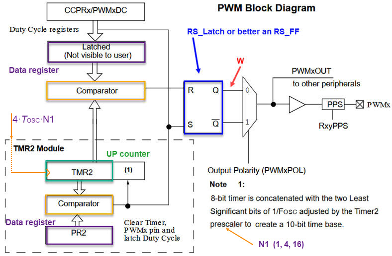
Discussion on the architecture. Thee PWM module will be conceived as an adaptation of the PWM-TMR2 Microchip PIC18F diagram copied in Fig. 1. from the datasheet or from this technical brief reference: Barbulescu, G., Bujor, I., "TB3270: Getting Started with PWM Using CCP on PIC18", Microchip.
|
|
|
Fig. 1. The initial idea on generating PWM waveforms: the PWM module associated with TMR2. The output wave is generated setting and resetting a simple RS latch cell. TMR2 comparator will drive S, establishing the waveform period (WP) determined by the value stored in PR2. Another comparator, by means of the duty cycle register will drive R configuring the pulse width (PW). |
From Microchip architecture in Fig. 1 we can imagine the symbol and the way the PWM is generated from the circuit's time base derived from the DE10-Lite 50 MHz crystal oscillator.
PW and WP parameters are linked, and thus the frequency of the waveform and the duty cycle (DC) resolution. For instance, WP = 1000 (10-bit), allows 0.1% resolution or up to 1000 DC increments. If we fix WP = 100 (7-bit) we obtain 1% DC resolution (100 steps).
Furthermore, the board's 50 MHz oscillator determines the maximum frequency generated for a given DC resolution. For example, if 0.1% DC resolution is required (10-bit or 1000 DC levels), the counter has to count up to 1000 every period: fPWM_outmax < 50 kHz. However, if only 6.25% DC resolution is required (4-bit or 16 DC levels): fPWM_outmax < 3.125 MHz. In this way, such peripheral can be adjusted for a wide range of applications.
For our LED lamp control, the signal frequency has to be high enough for the eye not to perceive the flicker. We propose fPWM_out = 1 kHz. Hence, for 0.1% DC resolution: fCLK = 1 MHz, requiring a CLK_Generator circuit dividing by 50 the OSC_CLK_in. On the other hand, if we accept only 16 DC values for our lamp, the CLK_Generator will divide by 3125 to obtain the required fCLK = 16 kHz.
|
|
|
Fig. 2. Symbol and the main components on PWM generation. |
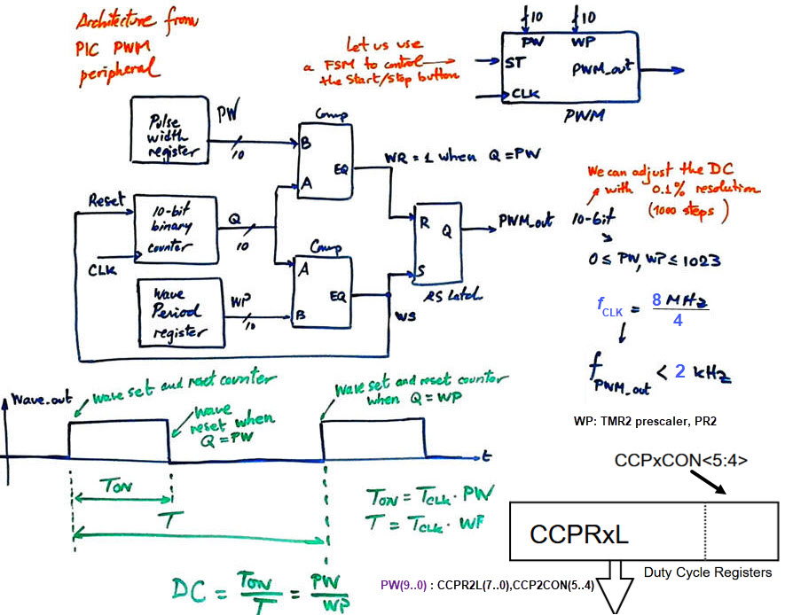
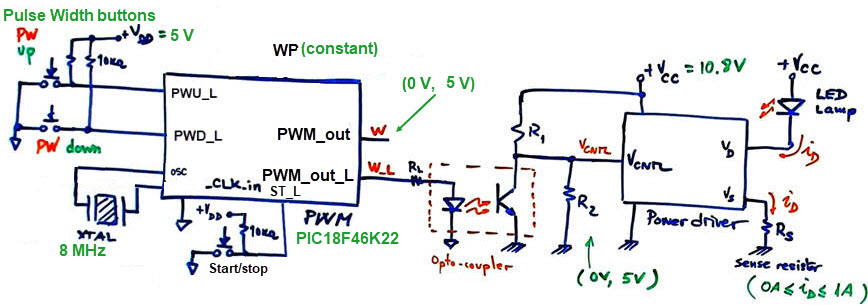
Fig. 3 shows how the PWM_top drives the optocouple and the lamp.
|
|
|
Fig. 3. PWM_top circuit for controlling the light intensity of the LED lamp. The PWM waveform is connected to the power driver using a phototransistor coupler adapting control voltage levels at the same time. |
| Specifications | 2. Planning | Developing | Test functional | Test gate-level | Prototype | Report |
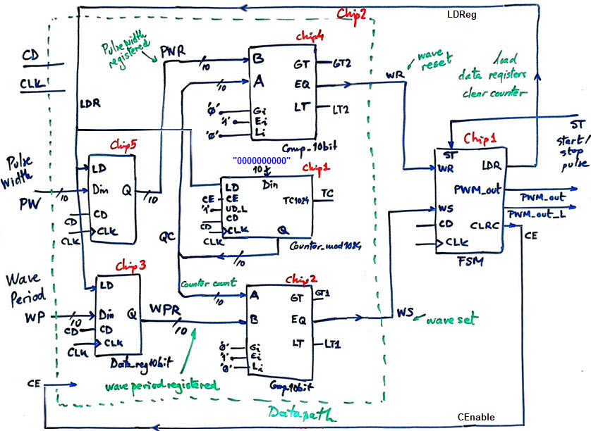
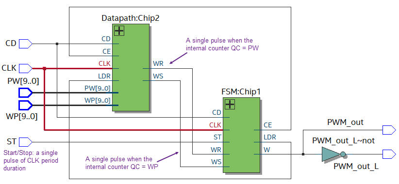
Design phase #1: As shown in Fig. 4, we can start preparing a VHDL-ready schematic for the basic PWM module using our library of components from CSD. The FSM will drive PWM_out and control the datapath from the status signals WR and WS and external start/stop pulses ST.
 |
|
Fig. 4. Circuit schematic ready for VHDL translation. Let's add the inverted output for driving active-low or active-high LED. |
The top circuit will provide a mechanism for generating a clean single pulse when clicking the start/stop push-button (debouncing and synchronising circuit). In the same way that it will provide the CLK_Generator for establishing CLK frequency.
As shown in Fig. 5, we can deduce the output waveform PWM_out equations.
|
|
|
Fig. 5. Example timing diagram and DC calculation. We will adjust the final formulas to calculate the wave period and its duty cycle after developing and testing sections; for the start button and the FSM will introduce some additional states. |
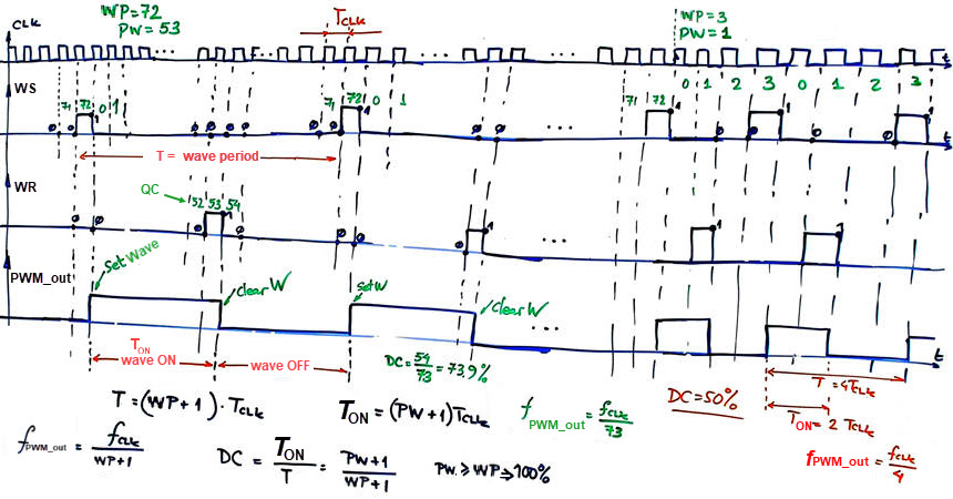
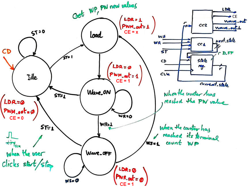
Fig. 6 presents the state diagram for the FSM.
|
|
Fig. 6. State diagram to control the datapath and generate the output waveform. The status signals from the datapath WR and WS indicate when to switch the waveform OFF and ON. |
Project location:
C:\DEE\Dimmer\FPGA_PWM\(files)
| Specifications | Planning | 3. Developing | Test functional | Test gate-level | Prototype | Report |
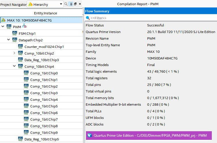
Let us translate the architectures above in Fig. 4 into VHDL: "PWM.vhd", "Datapath.vhd", "FSM.vhd", along with the internal components adapted from our library of products "Comp_10bit.vhd", "Comp_1bit.vhd", "Counter_mod1024.vhd", "Data_reg_10bit.vhd", create a new Quartus Prime project (PWM_prj) for the target MAX10 FPGA available in the DE10-Lite board, and synthesise the dedicated processor.
|
|
Fig. 7. Resources used and the RTL view of the synthesised project. 32 D_FF are required. 20 D_FF for the two data registers, another 10 D_FF for the counter, and 2 D_FF for encoding the FSM states in radix-2 (sequential). |
| Specifications | Planning | Developing | 4. Test functional | Test gate-level | Prototype | Report |
For simulations at this initial design stage, we will assume that ST is a short pulse of a duration similar to the CLK period, thus, it will be sampled high only one time per CLK period to emulate the state diagram.
Fig. 8 shows the VHDL testbench fixture "PWM_tb.vhd".
|
|
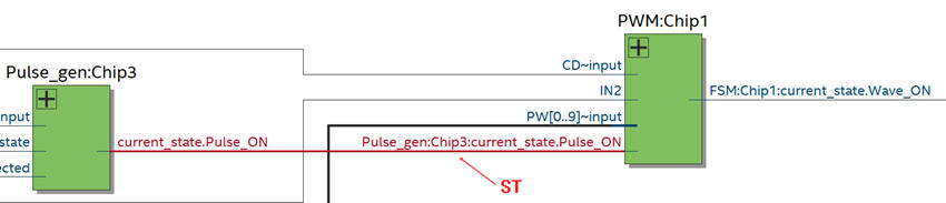
Fig. 8. Testbench fixture. To facilitate the debugging process, the functional simulation allows you to include in the visualisation internal signals such current_state, next_state, WR, QC, etc. |
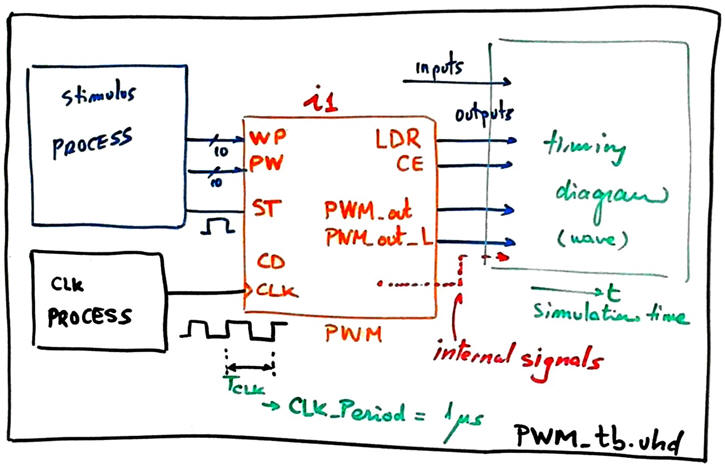
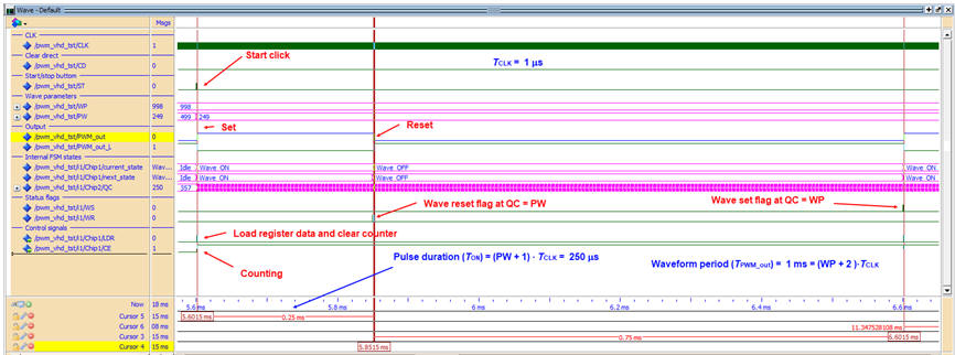
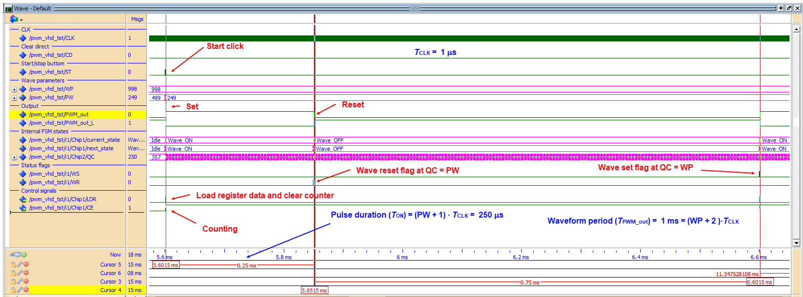
Fig. 9 shows the waveforms for the given parameters: TCLK = 1 µs, PWM_out period = (WP + 2)·TCLK = 1 ms, Pulse width = (PW + 1)·TCLK = 250 µs. This is a duty cycle DC = (250/1000) = 25.0 %. Using this architecture we can attain a DC variation from 0.1% to 100%, 10-bit resolution. And, because the OSC_CLK_in is 50 MHz, we can modulate at this resolution signals up to 50 kHz.
|
|
Fig. 9. Functional simulation using a testbench to drive both, oscillator and push-button clicks. |
This is the full project "PWM.zip" to be opened in Quartus Prime and ModelSim.
| Specifications | Planning | Developing | Test functional | 5. Test gate-level | Prototype | Report |
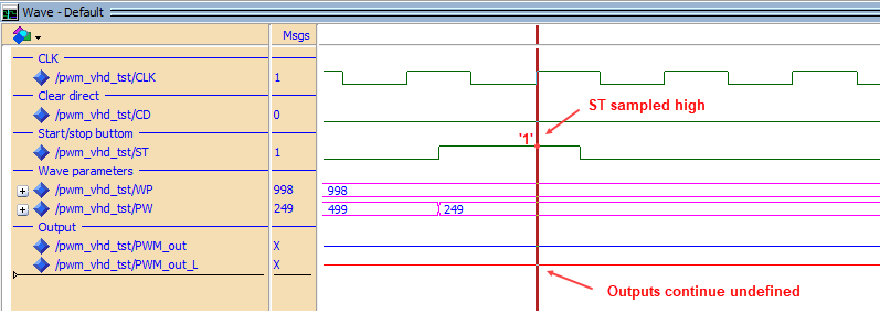
It is worth noting that the gate-level simulation, even if you are simulating only the ideal technology schematic circuit ".vho" without including the delay file ".sdo", does not work as expected. Why may be the reason?
| a) b) |
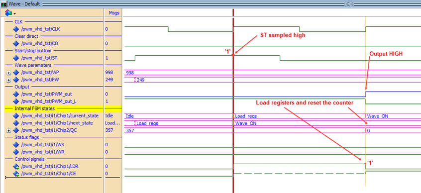
Fig. 10. a) Functional results when the ST is sampled high to start operations. b) Gate-level unexpected wrong results at the same CLK edge; outputs are not defined any time. |
Because we intent to prototype the circuit, it is better to follow up adapting the PWM_top to the DE10-Lite, as proposed in the next section.
| Specifications | Planning | Developing | Test functional | Test gate-level | 7. Prototype | Report |
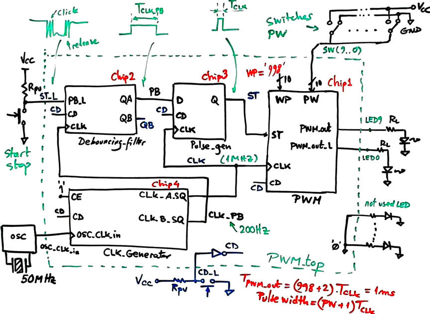
Design phase #2: PWM_top to interface the DE10-Lite switches and push-buttons.
Specifications
-
Let us add the clock generator to take advantage of the boards 50 MHz quartz crystal oscillator. In this experiment the aim is TCLK = 1 MHz.
-
Let us condition the start/stop signal from an external push-button ST_L. This means generating single filtered synchronous pulses to drive the dedicated processor.
-
Let us use the board 10 switches to fix PW values to program the duty cycle. WP will be set internally at 998 (1000 steps); it can be changed re-synthesising the circuit.
Planning
Fig. 11 shows the proposed top schematic.
|
|
Fig. 11. Enhanced diagram PWM_top, including the CLK_Generator and the debouncing filter and pulse generator to be able to synchronise start/stop pulses from the external push-button ST_L. Whatever click will produce a single synchronous pulse of fixed width TCLK. |
Project location:
C:\DEE\Dimmer\FPGA_PWM_top\(files)
Development
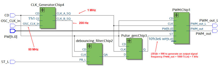
We need to use and adapt again circuits from CSD products. This is the page to copy the Pulse_gen. The CLK_Generator standard structure adapted from L8.2 is used to synthesise the CLK (16 kHz) and the CLK_PB (200 Hz).
|
|
Fig. 12. The RTL view. |
The full project "PWM_top.zip".
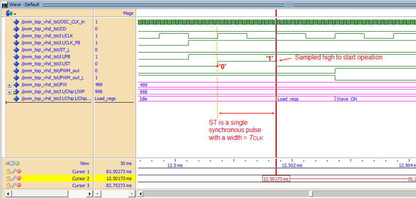
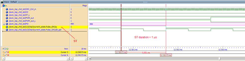
Test functional
We can visualise this experiment using both, functional and gate-level simulations, which this time it works as expected even if it takes a long time to simulate and get results.
|
|
Fig. 13. Functional simulation. |
|
|
Fig. 14. Gate-level simulation working correctly. Internal signals must be selected using the synthesised technology schematic. What is the reason that this time the circuit simulation works correctly? |
Test using the prototype
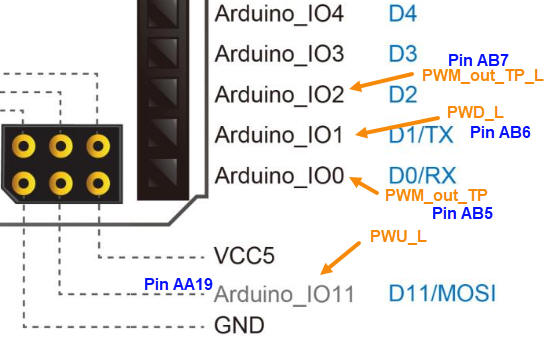
Now we can assign pins "PWM_top.csv" as shown in Fig. 15 using the boards' user manual , and synthesise the project to obtain the output files for programming the FPGA: PWM_top.sof", PWM_top.pof". In this phase we can use the 10 switches to fix the PW value.
|
|
Fig. 15. Elaborated picture from the user manual indicating assigned pins. |
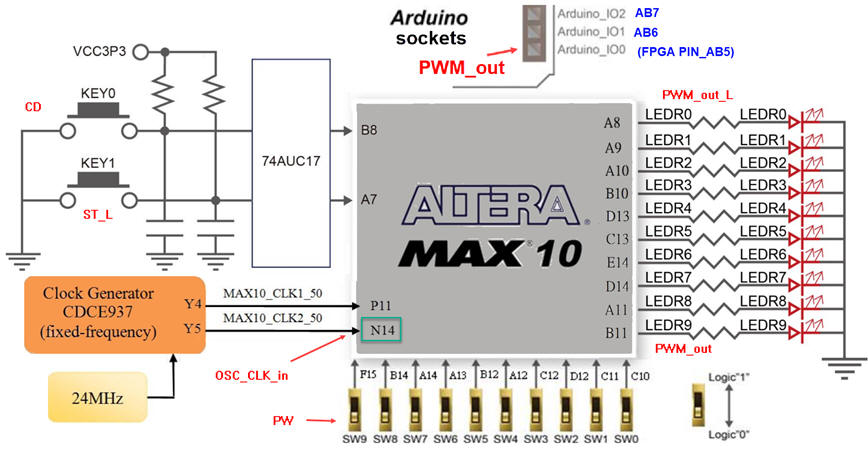
To make easier measurements in the lab we can replicate the PWM_out to a board's expansion socket, for instance PIN_AB5 connected to the Arduino IO0 signal.
|
|
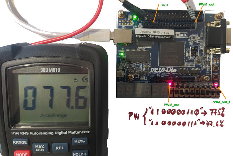
Fig. 16. Running the application. We can verify the 10-bit duty cycle resolution of 0.1% using the switches to increment PW. For instance, as shown in the picture PW = 775 ==> DC = 776/1000 = 77.6%. |
Design phase #3: Making easy the configuration of waveforms frequency and duty cycle.
Specifications
-
Let us add two push-buttons to fix the duty cycle up and down PWU_L, PWD_L. For instance, at maximum resolution, let us sweep all PW values in 5 s using the previous CLK_PB (200 Hz).
-
Now, let us use the board 10 switches to fix the WP value that sets both, the resolution and the signal frequency.
Planning
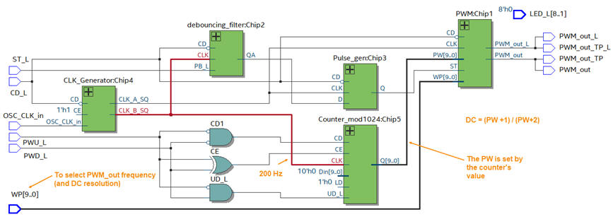
Fig. 16 shows the proposed top schematic that includes a new 10-bit up and down counter driven by the push-buttons.
|
|
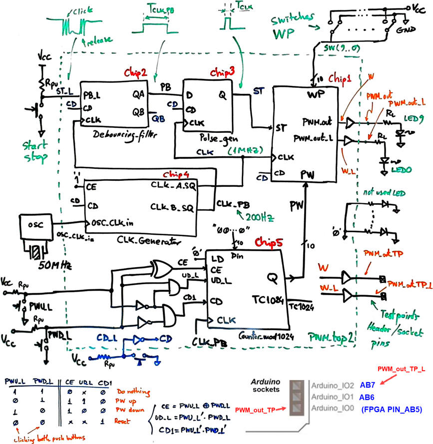
Fig. 16. The new PWM_top2 schematic. This parameter may be adjusted once the circuit running. The reversible 10-bit counter Chip5 activated by two push-buttons will set the pulse width. Using the CLK_PB frequency of 200 Hz, we can sweep all 1000 duty cycle values in 5 s. |
Project location:
C:\DEE\Dimmer\FPGA_PWM_top2\(files)
Development
In the same way we can translate all the circuits into VHDL, to generate a new project as shown in Fig. 17.
|
|
|
Fig. 17. The new version of the RTL to check that everything looks as planned. |
Test
We can solder two new buttons to control the counter up and down.
The full project "PWM_top2.zip".
|
|
|
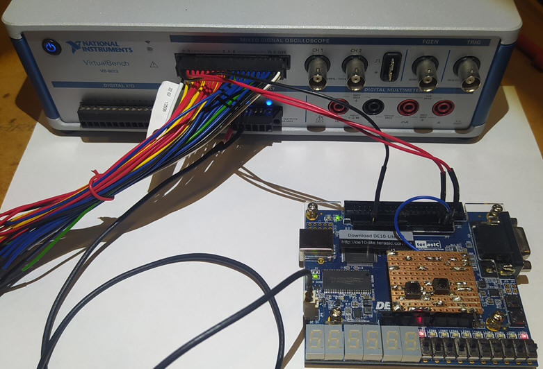
Fig. 18. Additional FPGA pins wired to convenient sockets used to interface the replicated outputs and also the new push-buttons. |
Assigning pins for the DE10Lite "PWM_top2_prj.csv", we can program the FPGA with the "PWM_top2.sof" or "PWM_top2.pof" to run the prototype. We can take a picture of the full circuit running, as represented in Fig. 17.
|
|
Fig. 18. Circuit running experimenting the PWM modulation of the light intensity. |
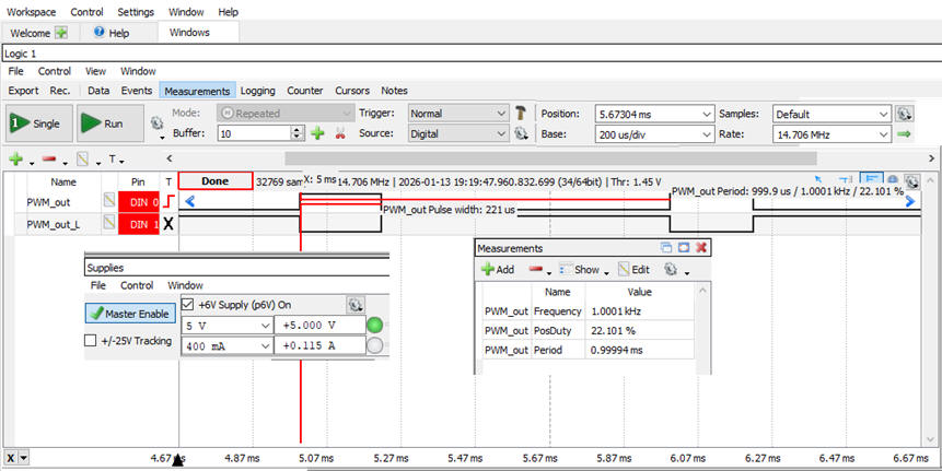
Using the compact instrument VB8012, we can capture the circuit waveforms and study their parameters.
|
|
Fig. 19. Measuring waveform parameters. |
Naturally, what is presented here in this tutorial page is only an starting point to fine tuning a given product; further modifications and enhancements are possible for this kind of applications. For instance:
-
How to relate the PW and the WP values, in a way that 0 ≤ PW ≤ PW - 1?
-
How to prevent the PW counter to overflow when clicking the duty cycle push-buttons for more than 5 s, or the same question: how to limit the duty cycle span from 0% to 100%?
-
How to sweep always all the PW values at the same 5 s rate, even if we lower the resolution (WP less than 10 bit)?
-
For precision applications, how to adjust both parameters using rotary encoders? How to visualise frequency and duty cycle using 7-segment displays?
-
How to reach the maximum frequency with 2-bit duty cycle modulation (25%, 50%, 75%, 100%)?
| Specifications | Planning | Developing | Test functional | Test gate-level | Prototype | 6. Report |
As you can see, the purpose of these pages is to show you examples on how to organise professional reports. Your aim is to design systematically, enhancing your product step by step. And, at the same time, publish quality technical materials and slides for public presentations. At this stage, you can continue your hardware design or switch technologies, proposing the same products using microcontrollers or other platforms.
| Home Contact Tutorials Electronic devices and companies Books Magazines Instruments Digsys Library EETAC DEEL |

|
|
| Web activa des de 01/2023, @ F. J. Robert. Web editat amb Microsoft Expression Web 4. El contingut és material de referència per al disseny d'equips electrònics. Llicència:Reconeixement 4.0 Internacional de Creative Commons |