|
Laboratory |
Laboratory 7 on synchronous counters plan Y, plan C2, plan X [P7] Plan Y: large FSM using STD_LOGIC_VECTOR signals and arithmetic libraries |
[21/11] |
| This is the group post lab assignment PLA6_7 to be submitted at Atenea before the due date. Study and execute in your computer this LAB7 and the previous LAB6 lab tutorials before attempting to solve this post lab assignment. |
2.7.3. Radix-2 binary counters (Counter_modM), large number of states
2.7.3.3. Design plan Y: designing counters using the VHDL arithmetic library and STD_LOGIC_VECTOR, single-file VHDL project
2.7.3.3.1. Example: Synchronous counter modulo 12 (Counter_mod12)
| 1. Specifications | Planning | Developing | Test functional | Test gate-level | Report | Prototype |
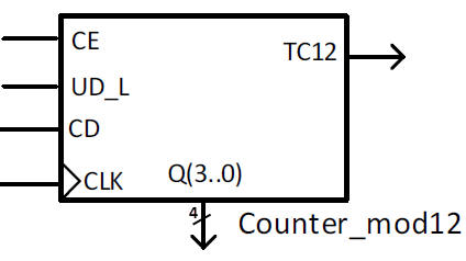
Design the synchronous counter modulo 12 (Counter_mod12) represented in Fig. 1 using plan Y.
 |
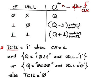 |
| Fig 1. Symbol and function table. |
|
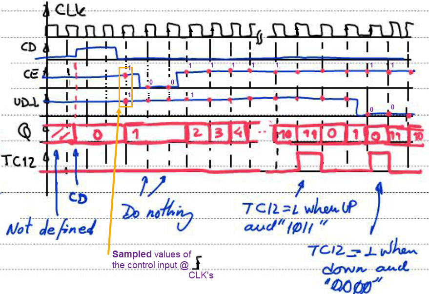 |
Fig 2. Example of timing diagram. |
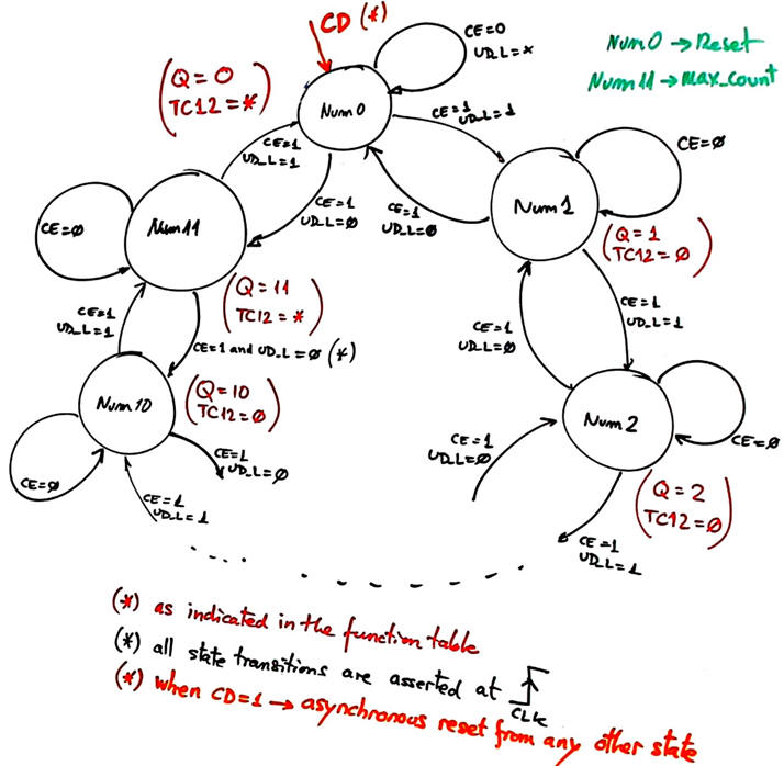 |
Fig. 3. State diagram representing the 36 state transitions and outputs. |
| Specifications | 2. Planning | Developing | Test functional | Test gate-level | Report | Prototype |
Let us plan this circuit as a FSM. The idea now is to use sequential (radix-2) encoding because the internal states will be simply buffered to the outputs.
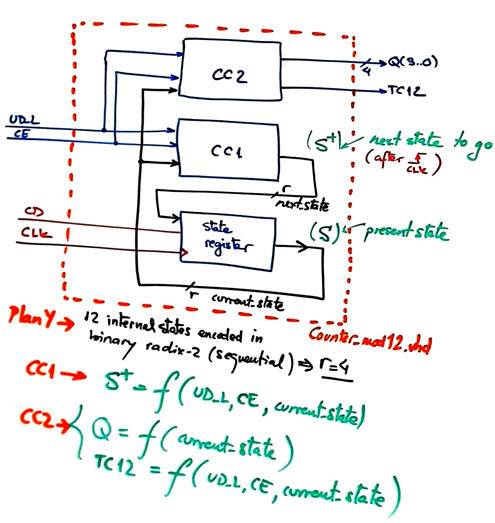 |
Fig. 4. FSM architecture. |
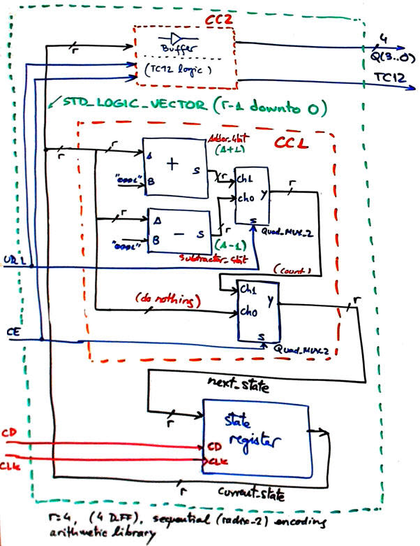 |
Fig. 5. FSM circuit to implement the Counter_mod12 using plan Y detailing the main ideas on CC2 and CC1 architectures. CC2 generates Q(3..0) buffering the internal state encoded in binary sequential (radix-2). It also implements the additional logic related to TC12. CC1 uses arithmetic blocks such as adders, subtractors and comparators to calculate the next state to go. Multiplexers are used to select between the several modes of operation. This circuit is easily scalable in VHDL because the internal states are configured as: STD_LOGIC_VECTOR(r-1 downto 0). |
Discussion for obtaining CC2 and CC1 truth tables and their equivalent flowcharts.
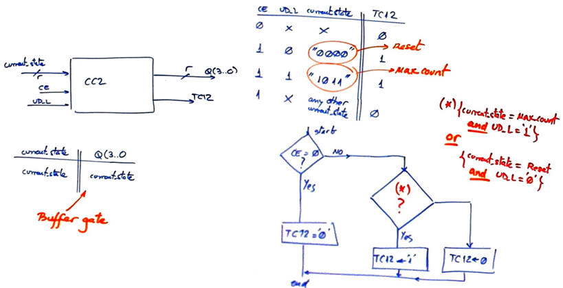 |
Fig. 6. CC2 truth table and flowchart. |
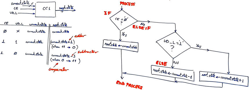 |
Fig. 7. CC1 truth table and flowchart where the equivalent translation to VHDL is inferred. |
Project location:
C:\CSD\P7\Counter_mod12Y\(files:Counter_mod12.vhd, etc. )
| Specifications | Planning | 3. Developing | Test functional | Test gate-level | Report | Prototype |
This is the Counter_mod12.vhd file that translates flowcharts in Fig. 6 and Fig. 7.
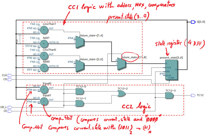 |
Fig. 8. RTL view with indications of the main components. This is how the synthesis tool interprets our ideas sketched in Fig. 5. |
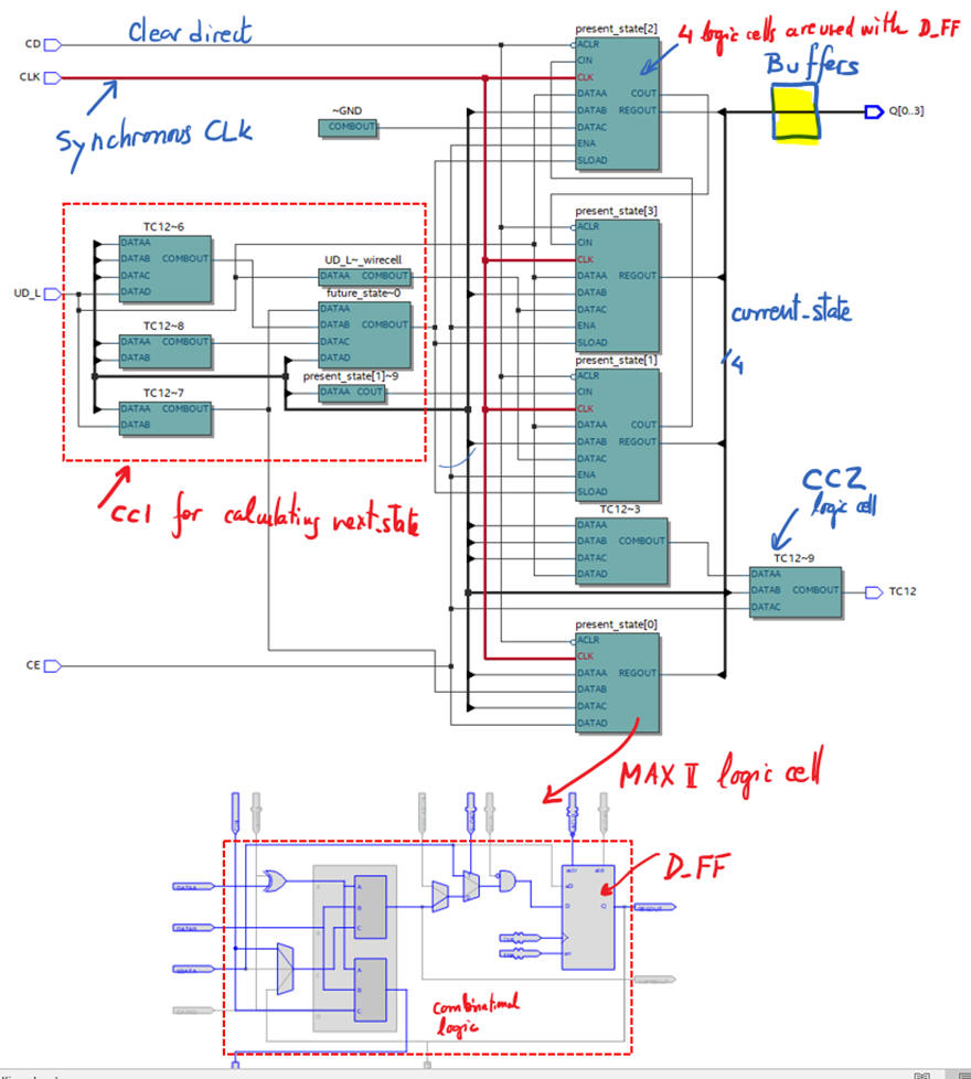  |
Fig. 9. Technology view schematic for a MAX II Intel CPLD and resources used (13 logic cells and 4 D_FF). |
| Specifications | Planning | Developing | 4. Test functional | Test gate-level | Report | Prototype |
Start the testbench template and add the CLK and inputs activity translating the timing diagram. Make all the timing relative to the CLK_Period constant.
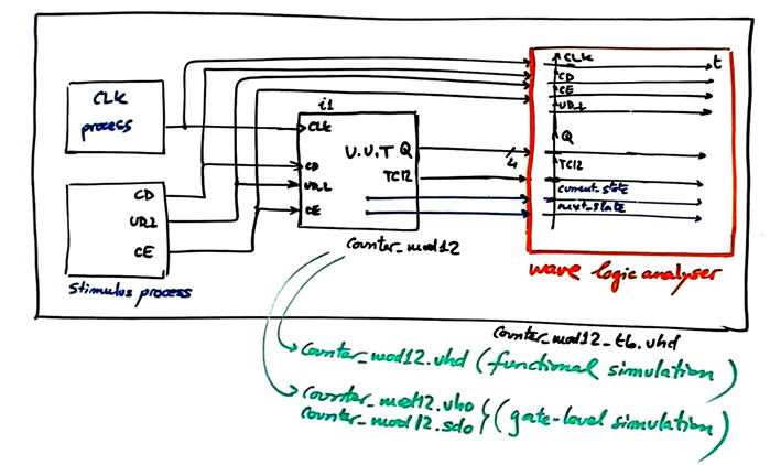 |
Fig. 10. Testbench schematic fixture. |
This is an example VHDL file translation from which you can copy the CLK_Period constant, and also the stimulus and CLK processes Counter_mod12_tb.vhd.
Functional simulation. Run the EDA VHDL tool and demonstrate how the circuit works adding comments to the printed sheet of paper containing the waveforms. Your system may works like the timing diagram discussed in class.
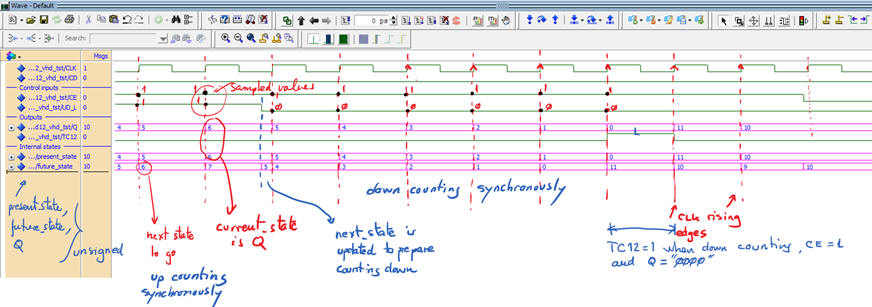  |
| Fig 11. Example of functional simulation of Counter_mod12. When running continuously (CE = '1'), TC12 is a periodic pulsed waveform that has a frequency fTC12 = fCLK/12 (frequency divider by 12). |
| Specifications | Planning | Developing | Test functional | 5. Test gate-level | Report | Prototype |
Gate-level simulations in ModelSim
Run the gate-level simulation of the project and measure the maximum frequency of operation. It is worth to know exactly which is the maxim CLK frequency for a given target CPLD or FPGA chip.
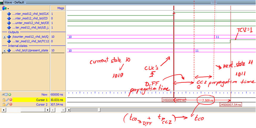 |
| Fig 10. Example of a gate-level simulation of the counter modulo 12 used to measure the parameter tCO in a given CLK transition. Target chip Intel MAX II. |
Quartus Prime timing analyser
Timing analyser spreadsheet to measure tCO. The extra logic for calculating TC12 represents a longer propagation time than for calculating Q(3..0).
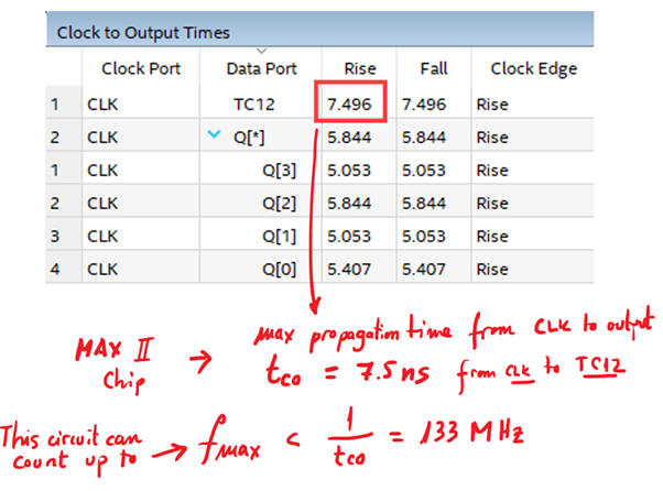 |
Fig. 11. Timing analyser spreadsheet for measuring tCO. |
| Specifications | Planning | Developing | Test functional | Test gate-level | 6. Report | Prototype |
Follow this rubric for writing reports.
|
Laboratory |
Laboratory 7 on synchronous counters plan Y, plan C2, plan X [P7] Plan C2: Hierarchical circuit on components and signals. Counter chaining and truncation. |
|
2.7.4. Count truncation and count expansion
2.7.4.2. Design plan C2: designing synchronous counters using hierarchical structures, standard components and logic, VHDL multiple-file project
2.7.4.2.1. Example of count truncation: Counter modulo 12 {Counter_mod12}
| 1. Specifications | Planning | Developing | Test functional | Test gate-level | Report | Prototype |
The same for plan Y and plan X designs. Pictures Fig. 1, Fig.2 and Fig. 3 represent symbol, function table, timing diagram and also the state diagram.
The idea if truncation and expansion is explained in this L7.3 lecture.
| Specifications | 2. Planning | Developing | Test functional | Test gate-level | Report | Prototype |
Hierarchical design using multiple VHDL files and components. The idea is truncating a larger counter like Counter_mod16 that is used as a building block. Discuss how this circuit works in Fig. 12. Study it for instance in two separate design steps:
- Step #1: Up counter considering only the CE control signal)
- Step #2: Add the UD_L control signal and discuss what blocks and logic has to be included in the basic design from phase 1 so that it becomes the circuit in Fig. 12.
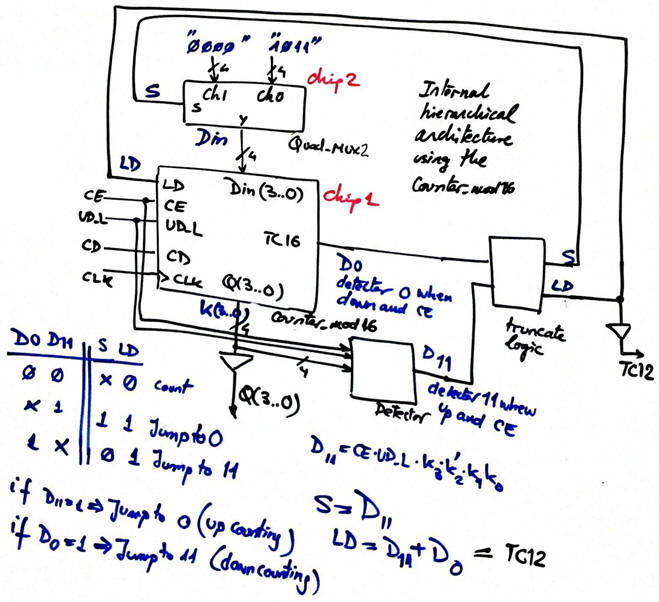 |
Fig. 12. Example of plan C2 circuit: Counter_mod12 implemented using standard Counter_mod16 building block. |
This is your project location:
C:\CSD\P7\Counter_mod12C2\(files)
| Specifications | Planning | 3. Developing | Test functional | Test gate-level | Report | Prototype |
These are the top Counter_mod12.vhd , and component Quad_MUX_2.vhd. In this tutorial there is the Counter_mod16.
Choose a MAX II device EPM2210F324C3 and start a Quartus Prime project.
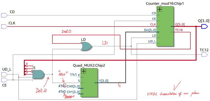 |
Fig. 13. RTL view translation of Fig. 12 schematic. |
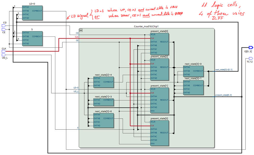 |
Fig. 14. Technology view schematic for a MAX II Intel CPLD. This plan C2 architecture is different from plan Y in Fig. 9, thus it will produce different propagation times. |
| Specifications | Planning | Developing | 4. Test functional | Test gate-level | Report | Prototype |
Running ModelSim and using the same testbench in Fig. 10 Counter_mod12_tb.vhd generates waveforms as in Fig. 11.
| Specifications | Planning | Developing | Test functional | 5. Test gate-level | Report | Prototype |
Gate-level simulations in ModelSim
Here is interesting to measure propagation times because we are proposing an alternative architecture that may be faster or slower than the one from plan X or plan Y.
 |
Fig. 15. Timing analyser spreadsheet for measuring tCO. |
Quartus Prime timing analyser
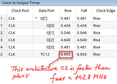 |
Fig. 15. Timing analyser spreadsheet for measuring tCO. |
Compare and discuss advantages and drawbacks for the same entity Counter_mod12 using these several design strategies.
From all these lessons on counters, truncation and expansion, it is not that difficult implementing for example a real-time clock HH:MM:SS or similar practical products. P8 is the unit devoted to advanced digital systems or dedicated processors.
| Specifications | Planning | Developing | Test functional | Test gate-level | 6. Report | Prototype |
Follow this rubric for writing reports.
|
Laboratory |
Laboratory 7 on synchronous counters plan Y, plan C2, plan X [P7] Plan X: Enumerated FSM as in P6. Only for a few number of states and state transitions |
2.7.2.5. Design plan X: designing counters as FSM for small number of states and any output code
2.7.2.5.2. Example: Counter_mod12 {Counter_mod12}
This is another example of P6 FSM enumerating states. This is the project location:
C:\CSD\P7\Counter_mod12X\(files)
|
Laboratory |
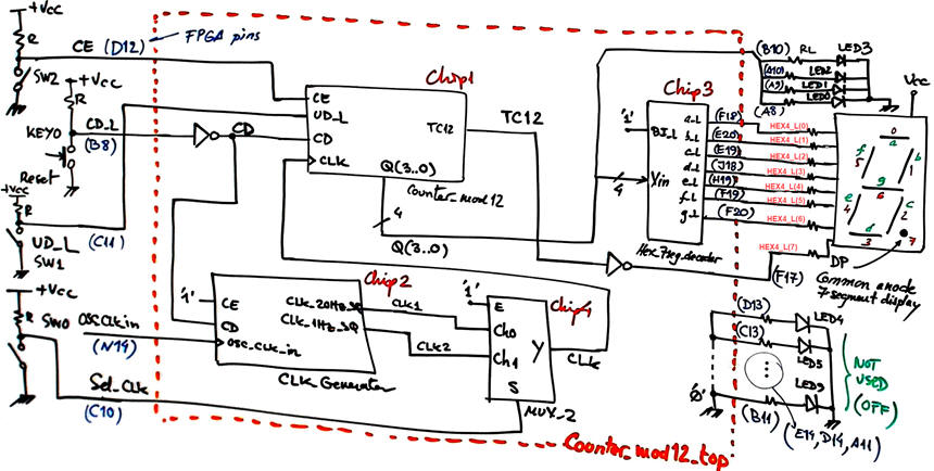
As a demonstration on how systematic and repeatable can be the idea of prototyping, we can develop in this lab tutorial the adaptation to the DE10-Lite board, similarly as we did in LAB6. This time we can run the counter from two CLK signals using a MUX_2 as represented in the Counter_mod12_top design in Fig. 16. Sel_CLK will select one of the two CLK sources provided by the CLK generator. This time we have to synthesise the project for MAX10 chip 10M50DAF484C7 installed in DE10-Lite board.
|
|
|
Fig. 16. Adapting the Counter_mod12 to the DE10-Lite board. Unused LED will be switch off. A new project Counter_mod12_top includes the additional blocks for interfacing the hardware. |
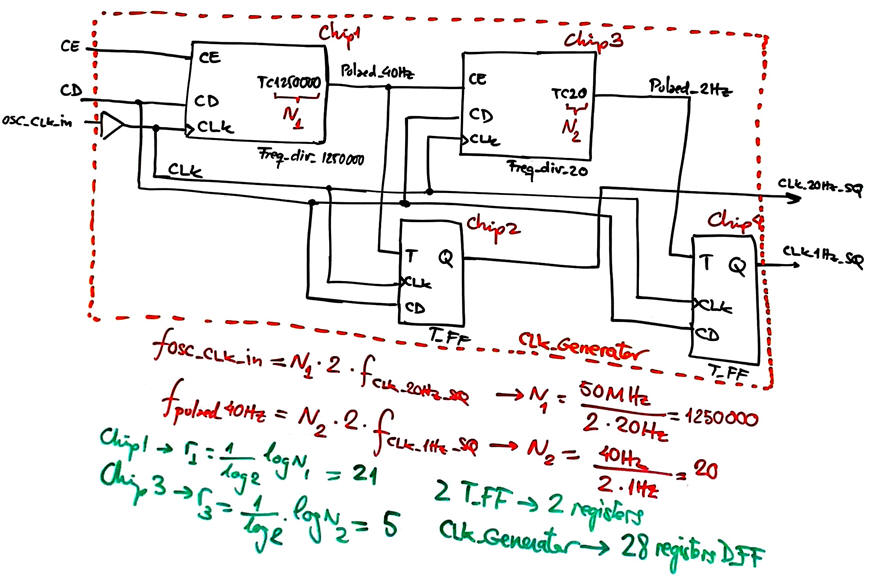
Fig. 17 shows the CLK_Generator.vhd schematic build using three internal components: Freq_div_1250000.vhd, Freq_div_20.vhd, and T_FF. Adapting the chainable modular architecture discussed in CLK_generator.
|
|
|
Fig. 17. Internal architecture of the CLK_Generator. |
This time, the Hex_7seg_decoder is used to show the counter's current count in one of the 7-segment displays (HEX4). And four LED(3..0) to show hexadecimal numbers from 0 to B are also included.
Using the MUX_2.vhd found in P2, we can complete the translation of the top schematic in Fig. 16 as Counter_mod12_top.vhd we can synthesise the project at the location:
C:\CSD\P7\Counter_mod12C2\DE10_Lite\(files)
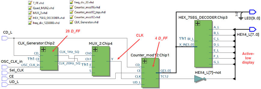
And inspect the RTL to check that everything is in place. Total number of D_FF registers in this application is 28 + 4 = 32.
|
|
|
Fig. 18. RTL view and list of VHDL files included in the project. |
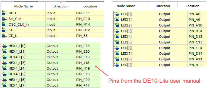
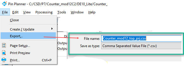
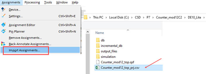
Pin planner tools in Quartus Prime allows you to fix LED, switches and 7-segment displays.
|
|
|
Fig. 19. Pin assignment list. It can be exported and imported using spreadsheet file extension. Counter_mod12_top_prj.csv |
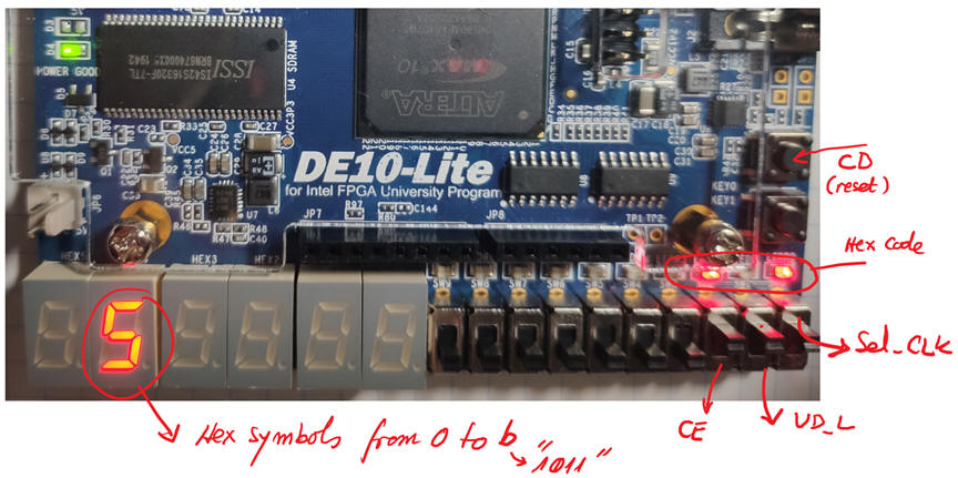
Programming the chip allows you to run the prototype with the current design. Check that the counter can be counting up, down or disabled. Check that it can work at any of the two CLK frequencies.
|
|
|
Fig. 20. Picture of the final prototype running the application. |
This is the final Counter_mod12_top.sof file to configure the FPGA using the programmer. This is the list of VHDL files Counter_mod12_top.zip included in this prototype.
Optional: See the debouncing circuit in action. Add a switch and another MUX_2 to the above prototype to allow you to input CLK pulses manually using the Key1 when selected.
Optional: Once plans X, Y and C2 are comprehended running these examples or similar ones, you may like to try inventing other counters and registers applying plan Y and plan C2 using our components Counter_mod16 (type 74ALS169) and Shift_reg_4bit (type 74HC194HC194).
Optional: Precisely, the highlighted project Hour_counter in P7 on a counter modulo 24 for counting hours is an example where we apply plan C2 techniques like counter truncation to obtain 24 states.


