|
|
Bachelor's Degree in Telecommunications Systems and in Network Engineering |
|
|
|
|||||
Chapter 3 problems |
- B3.15 - |
3-digit BCD to binary radix-2 converter |
B3.16 |
||
|
|
|||||
1. Specifications
Solve a 3-digit BCD to binary radix-2 converter using behavioural plan B ideas compiled for a PIC18F4520 μC.
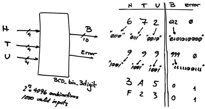
Draw and use the same BCD_bin_3digit circuit symbol in D1.15. Draw the truth table. Draw an example timing diagram providing some inputs and outputs. Find the conversion algorithm.
 |
|
Fig. 1. BCD_bin_3digit symbol and truth table. |
Draw an example of timing diagram to be used later as stimulus in the Proteus simulation of the circuit.
A) Planning hardware
Copy and adapt a circuit from any of the previous projects (LAB9) and name it BCD_bin_3digit.pdsprj. Assign pins to inputs and outputs accordingly to one of the following options (your instructior will tell you which):
Pin assignment option #1:
H(3..0) ---> RB(3..0)
T(3..0) ---> RC(7..4)
U(3..2) ---> RC(3..2); U(1..0) ---> RA(3..2)
B(9..8) ---> RB(7..6); B(7..0) ---> RD(7..0)
Error ---> RC1
Pin assignment option #2:
H(3..0) ---> RD(3..0)
T(3..0) ---> RB(7..4)
U(3..2) ---> RA(3..2); U(1..0) ---> RB(3..2)
B(9..8) ---> RD(7..6); B(7..0) ---> RC(7..0)
Error ---> RB0
Pin assignment option #3:
H(3..0) ---> RD(7..4)
T(3..0) ---> RC(3..0)
U(3..2) ---> RC(7..6); U(1..0) ---> RA(3..2)
B(9..8) ---> RD(3..2); B(7..0) ---> RB(7..0)
Error ---> RD1
Project location:
C:\CSD\P9\BCD_bin_3digit \(files)
B) Planning software
Organise the main program in our CSD way.
Propose a hardware-software diagram naming all the electrical signals, RAM variables and the software functions.
Describe all the RAM memory vairables used in this project and its type. How many bytes does var_B occupy?
Explain how to configure the µC in init_system(). List all RAM variables required and their type.
Organise using a flowchart the interface function read_inputs(). Include also the error detection when an illegal input is polled.
Organise using a flowchart the interface function write_outputs().
Infer the truth_table() software function using a behavioural interpretation and the corresponding flowchart.
Developing & testing (debugging)
Develop and test (debugging) the project capturing the hardware circuit in Proteus and writting the C source code.
| Note: Step-by-step tactical approach for developing and testing the project: Read one input at a time and run to check that the voltage value is correctly captured as a valid digital value in RAM memory. Write one output at a time and run to check that your code is correct; the output pin have the correct digitl value, for example turning on or off a LED. |
Write the BCD_bin_3digit.c source code translating the function flowcharts. Start capturing only one input as in (LAB9) and visualising it in the watch window. And only then go step by step developing & testing more inputs.
Start a software IDE project for the target microcontroller PIC18F4520 and generate the configuration files ".cof" and ".hex" after compilation. Discuss the project summary: % of ROM used for the code, number of RAM bytes used, etc.
Add a few lines of code every time, compile and run the test intereactively to check results watching variables.
Measure how long does it take to run the main loop code when using a 4 MHz and a 16 MHz quartz crystall oscillator.
| Home Term 23/24-Q2 Contact Products Electronic devices and companies Software Books Magazines Instruments DEE Library EETAC DEEL |

|
|
| Web activa des de 09/2001, @ F. J. Robert, J. Jordana. Web editat amb Microsoft Expression Web 4. El contingut és un complement als materials d'estudi del curs Circuits i Sistemes Digitals disponibles al campus digital Atenea. Llicència:Reconeixement 4.0 Internacional de Creative Commons |