|
|
Bachelor's Degree in Telecommunications Systems and in Network Engineering |
|
|
|
||
|
|
Analysis of a synchronous circuit |
|
|
|
||
(update)
LAB5 PROJECT PROPOSAL SAMPLE: Circuit_Sync1
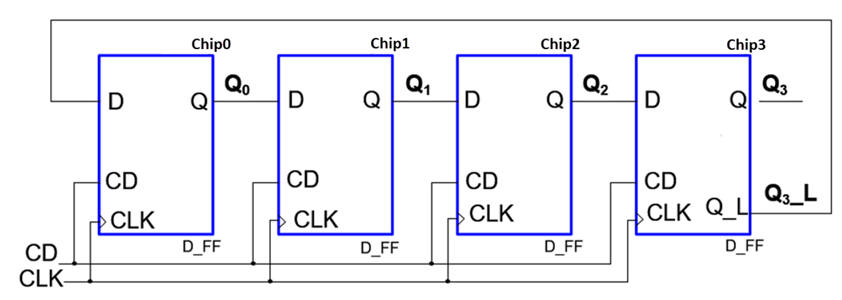
The circuit represented in Fig. 1 is composed of D_FF. Let us deduce how it works, how many states does it have and what may be its application. Synchronous structures are much more simple to analyse than asynchronous circuits because all registers are driven by the same and only CLK signal. These circuits will be systematically designed following our FSM approach presented in P6.
 |
|
Fig 1. Circuit_Sync1 to be analysed using up to three methods. Draw this circuit in you own sheet of paper. |
Phase 1: analyse the D_FF memory cell component.
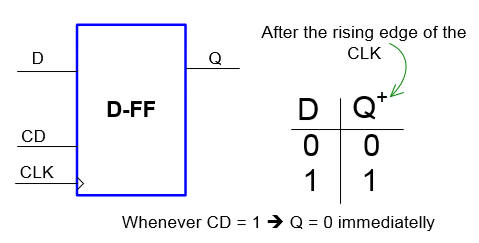
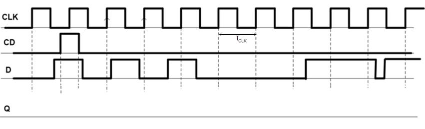
a) Analyse the behaviour of D_FF in Fig. 2 and represent the output Q in a timing diagram like the one represented in Fig.3.
 |
|
Fig 2. D_FF symbol, function table and state diagram. |
Indicate always the D sampled values using dots.
 |
|
Fig 3. Example input waveforms to be used as stimulus for calculating the output Q. |
Phase 2: circuit analysis. Three methods proposed.
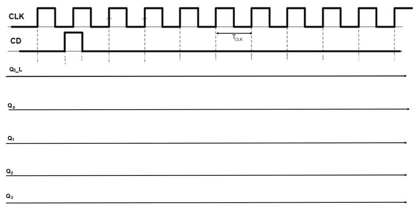
b) Method 1: Handwritten pen-and-paper analysis and discussion. Deduce the output Q(3..0) of the circuit represented in Fig. 1. The procedure is presented in P5 highlighted project.
 |
|
Fig 4. Waveforms. |
This method is developed in paper and results are verified by comparing with other methods.
Discuss how many states the system is capable of memorising.
Discuss what may be the function or application of the circuit.
This is an example of problem solution.
c) Method 2: using Proteus.
Capture Fig. 1 in Proteus and run simulations. For instance copy and adapt a similar structure such Proteus circuit based on CMOS classic chips. When picking parts from the library to mount your circuit, do this initialisation from Proteus top menu:
--> Tool --> Global Annotator --> Total.
Project location:
C:\CSD\P5\Circuit_Sync1\
Print and discuss results from the logic analyser.
d) Method 3: using VHDL synthesis and simulation tools (plan C2 circuit).
Get the component D_FF model and translate to VHDL the top circuit (Circuit_Sync1.vhd) to be able to start a new multiple-file plan C2 project.
Synthesise the project and print the RTL view. Be aware that the "number of registers" in the project's summary spreadsheet must be "4".
Prepare and use a VHDL testbench to demonstrate that the timing diagram looks like that obtained in Proteus or in the paper analysis above.
How can you measure the maximum speed of the circuit for a given target PLD?
Optional: Design exercise
e) Design an FSM that generates the same output Q(3..0).
| Home Term 26/27-Q1 Contact Products Electronic devices and companies Software Books Magazines Instruments DEE Library EETAC DEEL |

|
|
| Web activa des de 09/2001, @ F. J. Robert, Web editat amb Microsoft Expression Web 4. El contingut és un complement als materials d'estudi del curs Circuits i Sistemes Digitals disponibles al campus digital Atenea. Llicència:Reconeixement 4.0 Internacional de Creative Commons |